Hmmm. So that's +1.6 volts with pin 5 being the most positive (red lead on pin 5). IC's are usually super reliable so that is very odd.
What I would do is switch off and then check continuity from pin 7 on the chip itself (not the board, the pin on the chip) to the leg of 270k resistor R8. Then check continuity from the other side of R8 to the positive supply.
Another quick way... check the voltages are identical on R8 and pin 7, and R8 and positive rail. Beyond that and we need to confirm the 270k isn't open circuit. If all that is good then we are looking at the chip being faulty... but its never the chip")
What I would do is switch off and then check continuity from pin 7 on the chip itself (not the board, the pin on the chip) to the leg of 270k resistor R8. Then check continuity from the other side of R8 to the positive supply.
Another quick way... check the voltages are identical on R8 and pin 7, and R8 and positive rail. Beyond that and we need to confirm the 270k isn't open circuit. If all that is good then we are looking at the chip being faulty... but its never the chip
It will help you understand what going on if you know how the comparator works.
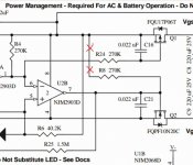
The comparator has two inputs, one marked - and one +, just like an opamp. In fact opamps can be used as comparators.
If the plus input is more positive than the negative input by even a fraction of a volt then the output swings 'high'. If the plus input is lower (more negative than the negative input) by even a fraction of a volt then the output swings low. That difference between the inputs need only be a millivolt or so for the comparator to work.
The output of this type of comparator needs a 'pull up' resistor in order for it to have a 'high' output state. That's R8 in this circuit.
Right, con checks.
Pin 7 to R8 is OK
The other leg of R8 to the positive rail (pin 8?) is a no go.
I used the PDF of the board to see where the trace should run and there is continuity from R8 to Q1 then Q1 to C15 then C15 to Pin 8. Although C15 to Pin 8 was a bit sketchy.
Would you suggest manually jumping pin 8 to R8 and trying again?
Thanks for the information on comparators by the way, im starting to take a real interest in electronics design and operation recently. All helps down the line
Thanks,
Michael
Erm this is where things get really really confusing. R8 is measuring minus 11.06V whereas pin 8 is measuring plus 11.61V.
Is there something I am missing here. I am reading both the board layout file and the schematic and I can see how R8 and Pin 8 are tied together. I am really confused how the voltage is swapping polarity over the length of a trace.
If it helps I am measuring -11.06 at Q1 too.
Is there something I am missing here. I am reading both the board layout file and the schematic and I can see how R8 and Pin 8 are tied together. I am really confused how the voltage is swapping polarity over the length of a trace.
If it helps I am measuring -11.06 at Q1 too.
Your not missing anything as such... and the polarity can't swap over along a trace... unless that trace has a break in it.
Now I've an admission to make and that is that I've never seen an O2 or the board for real, I work purely from the circuit diagram for all the fault finding in this thread.
What you need to do is look carefully at your board and try and see where pin 7 goes. Shining a torch through a PCB can be a good way to highlight traces. Favourite points for a trace to break are where a solder pad connects to the trace itself.
Q1...
That is the upper FET. There should be PLUS 12 volts on the 'source'. That's the left hand pin on the diagram. The gate (middle pin on the diagram) should be at MINUS 12 or so. Pulling the gate negative turns that FET on, so that is correct. In that state there should also be PLUS 12 volts on the right hand pin (the drain). The FET is on, it passes the 12 volts through to the rest of the circuit.
Does R8 have this MINUS 11 volts on both sides of it ???
Wow I never knew polarity could just swap.
If you have never seen an 02 before then this might help:
https://drive.google.com/file/d/0B52Awjeyc5zKMjRlYjlhNGItNGJlNC00ODlmLWIwM2MtNDI4ZWU4YWRjY2Y4/view
That has the circuit layout on it, might help I dont know if you had found that set.
R8 has minus 10.41 on the other side.
I am just going to quickly check for breaks.
Last edited:
It swaps because of a break. One point is now at a totally different voltage to the other.
Thanks for the link, its very fine print.
Just take it slowly. If R8 has MINUS voltage on both sides then the end that connects to pin 8 of U2 has a break somewhere.
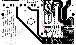
This looks to be the path.
Thanks for the link, its very fine print.
Just take it slowly. If R8 has MINUS voltage on both sides then the end that connects to pin 8 of U2 has a break somewhere.
This looks to be the path.
Attachments
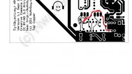
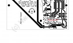
Hmm I really cant find the break, it might be hiding behind the silk screen or right on the solder pad.
I am pretty sure I know where the break is though. I have highlighted the trace in green.
I have also marked on the voltages at certain solder pads which indicate this trace to be the culprit.
Do you think it's worth breaking the trace at both ends and soldering on a wire as a replacement?
I am pretty sure I know where the break is though. I have highlighted the trace in green.
I have also marked on the voltages at certain solder pads which indicate this trace to be the culprit.
Do you think it's worth breaking the trace at both ends and soldering on a wire as a replacement?
Attachments
Last edited:
- Home
- Amplifiers
- Headphone Systems
- The Objective2 (O2) Headphone Amp DIY Project