Hello all,
After being delayed several times, i start a new thread about my new DIY project : a laboratory power supply.
I had already mentioned this project several months ago but without details.
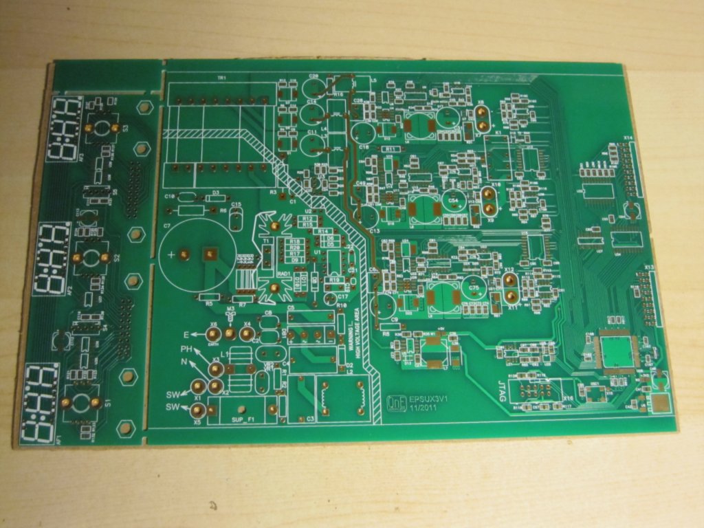
Now, the prototype PCB of this project has been made and the parts soldered.I must now test it and doing programming.
As many DIYers, i need to use power supply unit very often, for testing new electronics board, to repair hardware and for many others things...
So, i have compiled all my own needs for a PSU lab to design this new one.
It's main features are :
I will post soon some others documents (of course schematics and more).
Frex.
After being delayed several times, i start a new thread about my new DIY project : a laboratory power supply.
I had already mentioned this project several months ago but without details.
Now, the prototype PCB of this project has been made and the parts soldered.I must now test it and doing programming.
As many DIYers, i need to use power supply unit very often, for testing new electronics board, to repair hardware and for many others things...
So, i have compiled all my own needs for a PSU lab to design this new one.
It's main features are :
- AC input 90-250Vac 50/60Hz (no PFC).
- Resonant mode flyback design with low EMI signature.
- Low output noise design.
- High efficiency, low heat dissipation.
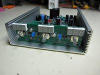
- Compact and light design, fitted in aluminium Hammond enclosure (1455T2201 - 220x165x52mm).
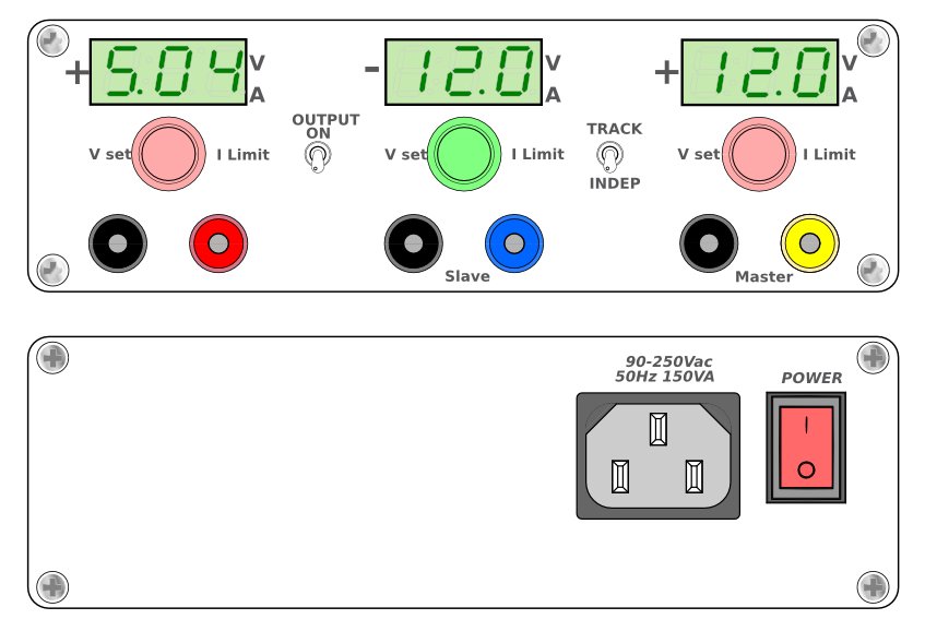
- 3 DC outputs with voltage and current limit adjustable.
- OUTPUT A : 2V....10V 0...3A max
- OUTPUT B : 4V....18V 0...3A max
- OUTPUT C : 4V....18V 0...3A max
- 100W max total output power.
- Each output is isolated and can be serialized (not same ground).
- 7 segments green led display for each output with digital encoder.
- Voltage and current adjustment.
- Current limit indicator.
- Enable all outputs switch.
- Tracking switch for OUTB/C for symmetric voltage adjustment.
- Minimal internal wiring.
- 4mm bananas outputs connector.
- CPLD based design for V/I control.
I will post soon some others documents (of course schematics and more).
Frex.
Hello all,
Nice work Cliffyk !
I hope to built a slightly small PSU for my lab .
.
Today i was working to design a test program for the PLD.
This program will allow to easily check all functions of the PSU controlled by the PLD,
like ADC, mux , digital potentiometers, 7 segments leds displays, rotary encoders and more.
I think to start these tests at the end of this week (i'm also very busy by my job).
As promised, i post the full schematics of the PSU.
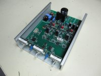
It's a un-debugged version, only a prototype board.
EPSUX3V1.1_sch.pdf
I will post all results as one goes along.
As you could see on the picture of the PCB, the power transformer is not yet soldered, i will build it and test the resonant flyback in a second step.
All design calculation will be also explain with expected and real waveforms.
To follow...
Frex
Nice work Cliffyk !
I hope to built a slightly small PSU for my lab
.Today i was working to design a test program for the PLD.
This program will allow to easily check all functions of the PSU controlled by the PLD,
like ADC, mux , digital potentiometers, 7 segments leds displays, rotary encoders and more.
I think to start these tests at the end of this week (i'm also very busy by my job).
As promised, i post the full schematics of the PSU.
It's a un-debugged version, only a prototype board.
EPSUX3V1.1_sch.pdf
I will post all results as one goes along.
As you could see on the picture of the PCB, the power transformer is not yet soldered, i will build it and test the resonant flyback in a second step.
All design calculation will be also explain with expected and real waveforms.
To follow...
Frex
Attachments
Last edited:
Test in progress...
Hi,
I have written a first software for test.
It allow to test many functions separatly and easily.
The PLD was succesfully programed with, and no big issue was encountered.
I must work hard now next week on the final PLD program that will include many more logics functions...
Frex.
Hi,
I have written a first software for test.
It allow to test many functions separatly and easily.
The PLD was succesfully programed with, and no big issue was encountered.
- 7 segments display multiplexing is ok
- Digital encoder's and leds are ok
- U/I mux and A/D converter is ok.
- All digital potentiometers (for setting V/I) are correctly drived,
- All bucks work fine with approximatively expected voltage range.
- Symetric control of outA/outB is ok.
- Output enable switch is ok.
I must work hard now next week on the final PLD program that will include many more logics functions...
Frex.
Hello,
Thank you 6M9, i just try to build PSU that fit well for my need with my own user feedback.
The CPLD program is now ok at 99%, i just need to use the internal EEPROM for record the last U/I settings for restoring these values at next strart-up.
As soon it's ok, i start to build the tranformer and test the flyback converter.
Some pictures or video will come...
Frex
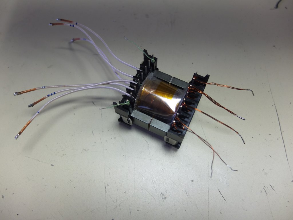
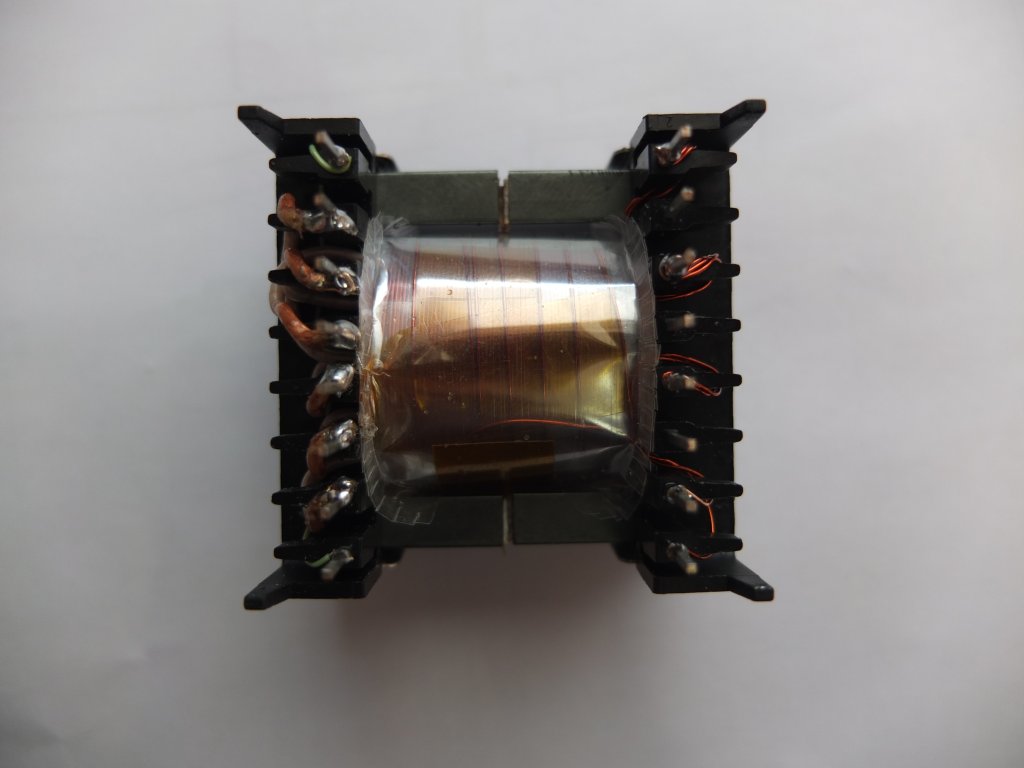
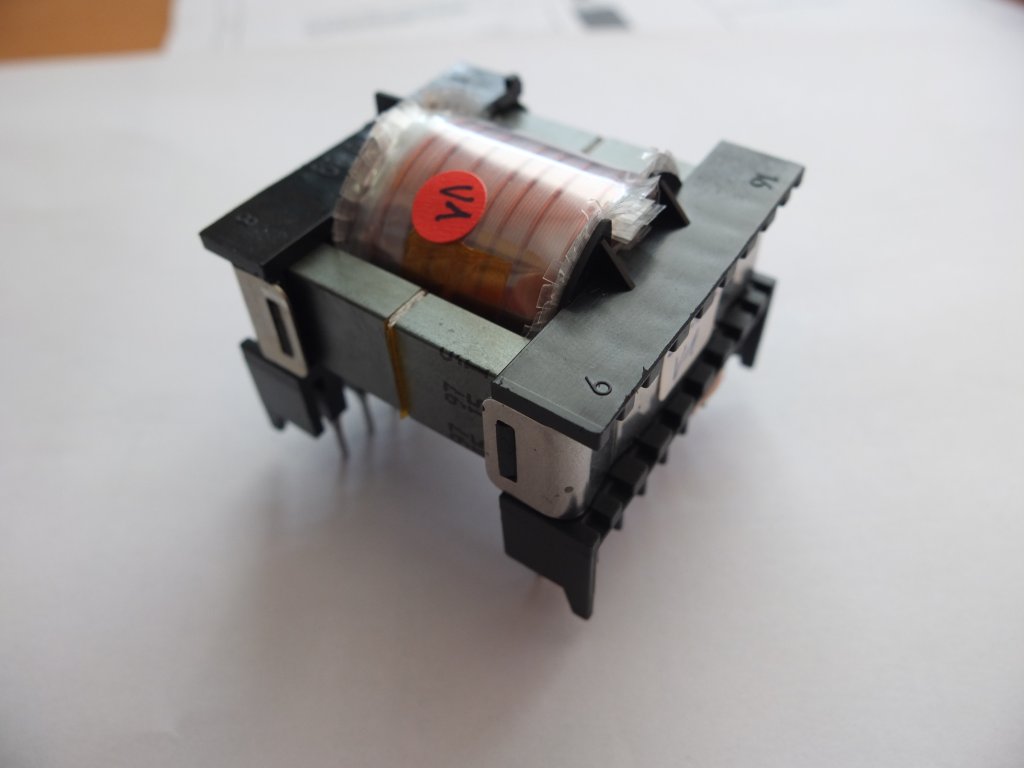
Hi,
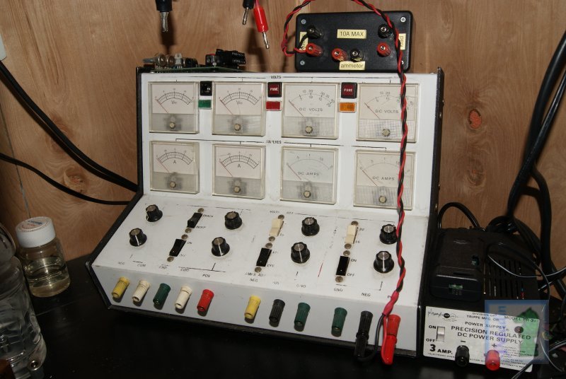
The flyback transformer prototype has been wound.
I test it's "real life" specs in the week with an "on the fly" test board.
The primary is split in 2 for lower leakage, and secondary windings are
winding at same time for maximum coupling.
I use Litz wires for secondary, but multiple small wire could work too.
In/out parasitic capacitances are neutralized with two copper shields between primary/secondary sides.
The shunt copper layer outside the transformer core that reduce radiated EMI will be added only
at the end( transfomer fully characterised).
Frex.
PSU resonant flyback of EPSUX3 first tests!
Hello,
I have made many tests with the prototype transformer and first results are very good.
I reach the full output power of 115W without problem at expected switching frequency with an overall efficiency of about 85%.
The "on the fly" circuit board for testing the transformer looks like this :
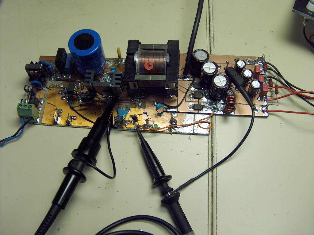
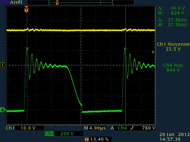
You can see below the voltage waveform at the Drain of primary switch(green),
that showing the turn-on near 0V confirming ZVS. The output voltage of one of the three outputs is in yellow.
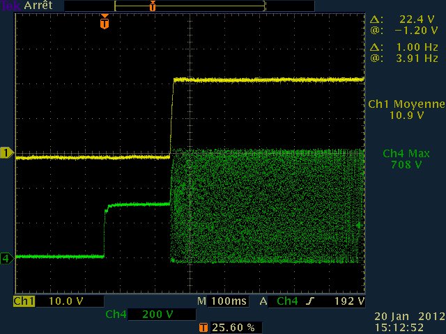
Here, it's the start-up sequence (yellow= output voltage, green Vds primary switch):
No excessive heat has been observed during max output power for long time, confirming
good transformer design.
I will now made several tests on it to define efficiency and loss charts, test it in short circuit condition, open loop and more. I will do also losses map.
all results will be posted.
I recall that the scheme is available HERE.
The old video demo of the front panel in working of EPSUX3 can been see HERE.
Comments welcome !
FRex
Hello,
I have made many tests with the prototype transformer and first results are very good.
I reach the full output power of 115W without problem at expected switching frequency with an overall efficiency of about 85%.
The "on the fly" circuit board for testing the transformer looks like this :
You can see below the voltage waveform at the Drain of primary switch(green),
that showing the turn-on near 0V confirming ZVS. The output voltage of one of the three outputs is in yellow.
Here, it's the start-up sequence (yellow= output voltage, green Vds primary switch):
No excessive heat has been observed during max output power for long time, confirming
good transformer design.
I will now made several tests on it to define efficiency and loss charts, test it in short circuit condition, open loop and more. I will do also losses map.
all results will be posted.
I recall that the scheme is available HERE.
The old video demo of the front panel in working of EPSUX3 can been see HERE.
Comments welcome !
FRex
Last edited:
- Status
- This old topic is closed. If you want to reopen this topic, contact a moderator using the "Report Post" button.
- Home
- Design & Build
- Equipment & Tools
- Triple outputs 100W Laboratory PSU -- A new DIY project .