Hi Coris, I'm thinking of upgrading the Elna 6800uf 35v Caps on the Analog board of 205 to Mundorf 22000uf 40v or 25v MLytic AGs and bypassing with a film cap. My question is ripple current Verses ESR.
The 40v version of the Mundorf has 8.5 Nominal ripple current IR at 105C and 100hz and an ESR value of 9ohm at 100hz.
The 25v version of the Mundorf has 5.4 NRC IR at 105C at 100hz and ESR of 14ohm.
The 63v has 11.2 NRC and 7ohm ESR. which I don't think will fit.
Can you tell me which would be more desirable to use in this area?
Thanks for your future response.
Moto.
Hi
You chosen right value for the filtering caps, but 40v rating is fully unnecessary (it may result a too big dimension). 25v is also a good choice. I will chose the lowest ESR. Also highest ripple current is all right. I think in your examples the ESR is quite strange too high. As usual, at this capacity value, the ESR it should be of teens mOhm, or so, but not ohms...
Not always the legendary brands capacitors are the best ones for the task...
Hi Guys,
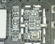
I need help! Can someone help please? When replacing the clock in analog board (100mhz), I accidentally broke the solder point (red circle in photo). Where else can I connect to new clock ? Can I connect to R605 left side?
Thank you
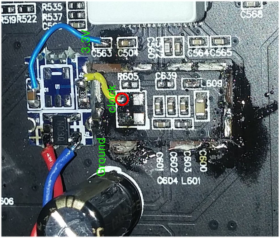
First I may say that removing the shielding can of the DAC oscillator (very difficult also), as removing the oscillator itself, it is highly unnecessary.
There is far easier cutting only the 3,3v power trace to the oscillator (inside the shielding), and the output clock trace (outside the clock shielding can). See picture. In this way the DAC clock is fully isolated. The insertion of the new clock signal it can be done in the remaining input clock trace, scratched accordingly and plated with soldering.
In your case. you can now remove R605, and insert there the new clock signal (pad connected to the DAC clock input trace).
Attachments
Last edited:
First I may say that removing the shielding can of the DAC oscillator (very difficult also), as removing the oscillator itself, it is highly unnecessary.
There is far easier cutting only the 3,3v power trace to the oscillator (inside the shielding), and the output clock trace (outside the clock shielding can). See picture. In this way the DAC clock is fully isolated. The insertion of the new clock signal it can be done in the remaining input clock trace, scratched accordingly and plated with soldering.
In your case. you can now remove R605, and insert there the new clock signal (pad connected to the DAC clock input trace).
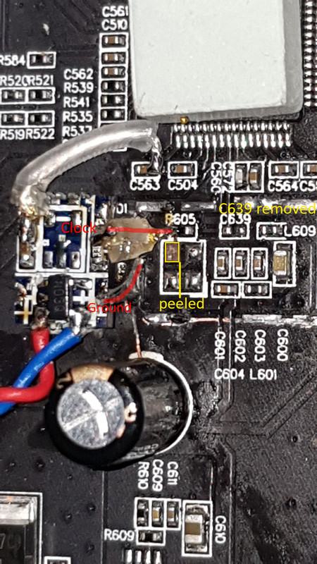
Thank you Corris, but can you be more specific? The PCB photo you attached looks different than mine. Mine is 205 analog board. I have opened the can and remove the original clock. Opening the can was a bitch!!
I supposed to connect the clock to the red dot but I peeled the plated!!
Right now I connect the clock to R605 left side (R605 still intact) and so far it is working. Here is a close up photo for guidance (not real photo of my MOD). C639 was removed.
Last edited:
Opps correction ") mohm not ohm.
mohm not ohm.
Coris, thank you, I actually was reading the data sheet incorrectly it was mohm. I'm ordering the 25v piece, it will fit nicely.
https://www.partsconnexion.com/media/pdfs/mundorf_ag.pdf
Moto
mohm not ohm.Hi
You chosen right value for the filtering caps, but 40v rating is fully unnecessary (it may result a too big dimension). 25v is also a good choice. I will chose the lowest ESR. Also highest ripple current is all right. I think in your examples the ESR is quite strange too high. As usual, at this capacity value, the ESR it should be of teens mOhm, or so, but not ohms...
Not always the legendary brands capacitors are the best ones for the task...
Coris, thank you, I actually was reading the data sheet incorrectly it was mohm. I'm ordering the 25v piece, it will fit nicely.
https://www.partsconnexion.com/media/pdfs/mundorf_ag.pdf
Moto
Coris,
It is 2AM here, I cant sleep and opened my 205.
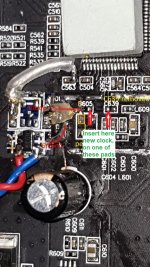
Here is the actual photo. Clock was supposed to go to peeled section but now I connect to R605 instead. C639 was removed per install instruction. Can you help for the best solution?
Thank you
Well, I do not think it are differences when about the can content. I see you have added a small PCB right beside the clock circuits.
You can still use the pad of R605 to inject the new clock signal.
However, I maintain my recommendation not messing up with can removing and original oscillator, as it is unnecessary and enough risky (as you already experienced). Well, you have done it, so my recommendation is directed to the resto f DIYers...
Attachments
Last edited:
Well, I do not think it are differences when about the can content. I see you have added a small PCB right beside the clock circuits.
You can still use the pad of R605 to inject the new clock signal.
However, I maintain my recommendation not messing up with can removing and original oscillator, as it is unnecessary and enough risky (as you already experienced). Well, you have done it, so my recommendation is directed to the resto f DIYers...
Hi Corris,
I appreciate you feedback. C639 was removed, so only option is R605? Does the left and right of R605 have different circuit? I'm connecting to the left side now and it is working. Does changing to the right side will have more benefit?
Thank you so much!
I had the impression (out of your picture), that you have removed R605. Therefore I suggested as in my last picture. If you have already connected to the left pad of R605, and it is working, then it mean the resistor it was not removed. In this case the clock signal goes through R605. If you will insert the clock signal as pointed in my last picture (actually your picture), then the clock it may be of a higher level (directly into the chip clock input pin.
If it could be better and less better, then some measurements on how the signal it looks like, should be taken. I think this is not so important, if the DAC it is running.
So, good luck further!
If it could be better and less better, then some measurements on how the signal it looks like, should be taken. I think this is not so important, if the DAC it is running.
So, good luck further!
Hi Den
You can short that resistor, but my advice is having a resistor there however (10 - 50 ohm). Eventually moved on the downside of the board. The meaning of that transistor its to adapt the output stage to the cables (or the opposite). Also that resistor it reduce the capacitive load seen by the last opamp output.
The impact of that resistor on signal quality is minimal. Much important (decisive) impact over signal quality it have lot of factors before that resistor...
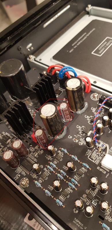
Hi Coris,
I have spare Blackgates 4700uf 16V, can they replace these caps rated 25v and 50v (see in photo red line)? Are these 3 for XLR output and the most right one for 7.1 board?
I disconnect the 7.1 board, I will only use XLR out.
Lastly, is it safe to replace XLR's output caps 100uf one with 2.2 uf film caps? I have unused clarity caps CMR.
Thanks
The two (dimensional) small caps beside the big one in the middle (as marked in your picture), it can be safely replaced by 16v rated ones. The big cap in your marked area, it can be 10v rated.
There is not a good idea replacing the 100µ coupling caps with only 2,2µ film or whatever. If it is about bypassing the 100µ caps with 2,2µ film, then this configuration is very recommended. You can off course try doing as you intend, to experience by yourself, that is not a good thing, heaving only the 2,2µ caps there...
The larger the capacity of the coupling caps, the better will pass through the low end of signal spectre.
The best way of doing there (coupling area) is just bypassing that coupling caps with a wire, if the DC offset on outputs is into 0 - 10 mV range. As usually it is so....
Hi Corris,
Thanks for the info.
I have more question for you. I want to replace +12V and -12V regulator in the analog board with low noise one.
Will this be okay? It has only 1.5 A maximum current.
Thanks
Output Voltage (Input = 18V no load) typ. 12.00Volts
Output Voltage (Input = 40V) typ.1 2.43Volts
Output Voltage (Input = 40V) max. 12.60Volts
Output Voltage (Input = 18V half load) typ. 11.98Volts
Maximum Input Voltage 40Volts
Maximum Current 1.5Ampere
Maximum Power drop (dry mount). (1) 4 watt
Watts Maximum Power drop (silicone grease mount). (1) 25 watt
Watts Dropout Voltage 2.5Volts
Peak Current (10mS) 10 ampere
Ampere Isolation Voltage to heatsink 750Volts RMS
(1) Power drop is calculated as: (Input Voltage - Output Voltage) * Load current. For example:
12V in 5V out and 0.5A load gives: 12 - 5 = 7 * 0.5 = 3.5W.
Last edited:
4+4 DAC config for dedicated balanced output
Hey Coris
In you experience with the Oppo 105 you may have mentioned that allocating 4+4 DAC chip outputs to the dedicated balanced output may be the best mod for sound - if one is not interested in headphone or RCA output.
Would this be true for the Oppo 205 ES9038PRO? Have you tried this?
Denis
Hey Coris
In you experience with the Oppo 105 you may have mentioned that allocating 4+4 DAC chip outputs to the dedicated balanced output may be the best mod for sound - if one is not interested in headphone or RCA output.
Would this be true for the Oppo 205 ES9038PRO? Have you tried this?
Denis
Hi Denis
Well, it is good you have pointed on this aspect. Actually my statement about 4+4 configuration of the DAC outputs is not quite right in this context. It is right when taking the Sabre chip alone, but in Oppo design is not possible a 4+4 configuration. I have also corrected my assertion in some following posts at that time.
So, a 4+4 configuration is not possible for the Sabre DAC chips in Oppo design. This is because Oppo have allocated 2+2 channels to the headphone output, 1+1 for XLR, and 1+1 to RCA. The channels for headphone it cannot be reconfigured, as these are muted by firmware, when the rest of the channels are active, and the opposite. For a 4+4 configuration, one need all the channels being active in the same time. The firmware it cannot be modified.
So, the available option is the 2+2 configuration (original XLR and RCA unified). This is possible in both model cases 105 and 205 as well.
I do actually this way (always unifying the two pairs of channels), when I install my output module. Also my module is compatible for both models.
So, as conclusion, Oppo design allow only a 2+2 configuration, and this is possible on both Sabre DAC versions (old/new).
Headphone output it benefit of two channels pairs (second 2+2 configuration), and this it cannot be changed (both models 105/205).
Last edited:
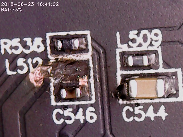
Hi Corris,
Can you help me? I just replaced all caps in the analog board with same value and something happened. XLR out has not sound and L512 in the main board blow up. I test optical out and it has sound, havent test HDMI out.
Can you tell me what is L512? What to replace and how to fix? We double check caps in the analog board and nothing is short and looks fine so I don't know what cause this.
Do you know where to get 205 service manual btw?
Thanks
Uhhh!! Not so good such things.
That line which the L512 is placed, it transport the main+12v from SMPS. So you may have a severe short on the main power line. The short is somehow after that L512. I suspect you got a short (+12v to ground) right on the flat cable which it transport that rail to stereo board.
I suggest you examine the flat cable connector. The contacts on that side of the connector it may be exfoliated, touching somehow the ground pin right beside (the last two pins of CN401 are allocated for +12v rail). Or the opposite it could happen as well (the GND pin touching the +12v rail pins). A ground pin in that connector is the third pin counting from that left side of the connector.
That flat cable is quite fragile on its connector area, and the receptacle of that connector is not the best one either. As you experimented much, and the flat cable had enough connecting/disconnecting cycles, its connector on the end it could be damaged, so to cause a short to ground for the main 12v rail.
I have already replaced that CN401 receptacle on my stereo board with another one, much better connector, which it easily tolerate many connecting/disconnecting cycles (attached picture).
If the +12v rail is not present at that pins (because the L512 it blow it up), then no any sound on stereo board)
The burning out of the L512 should not be connected to the caps replacement on stereo board. I think you were lucky this time that L512 it burned out (as a fuse).
If you may not have a new similar ferrite bead, then you can (temporary) bypass it with a wire or soldering together its pads. Else almost any ferrite bead it should work well in that place. You may chose one rated for at least for 500mA.
Good luck!
Attachments
Last edited:
This is the Mouser code for the FFC receptacle: 710-686130148922
When about the FFC cable, all the cables are good when are new. You should find a similar one, with almost the same length, same 1mm pitch and same number of wires. Or a wider cable and then cutting it accordingly. The receptacle is specified for a certain thickness of the cable end connector.
These cables and their end connectors, are not made for many connecting/disconnecting cycles. So, after a such use the connectors pads it get bad. However, the receptacle I recommended, it have another way of making contact (by perpendicular pressure - no any friction involved), which it preserve the connector pads quite much. On this connector the lid it get "tired" after many times using it. However, it hold longer enough and it provide a better connection.
Last edited:
- Home
- Source & Line
- Digital Source
- Oppo new UDP series players - 203/205 - Discussions, upgrades, modifications