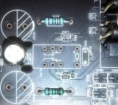
This is the XLR output on 205. Also all the outputs it have these diodes to ground, as similar components placed on the signal lines/path.
My guess is the diodes connected in between signal line and ground are meant as ESD protection.
A ferrite bead (placed on all the outputs signal lines) are meant to lower or filter out high frequency residual signals.
Any comments, more opinions, thoughts about such design and how safe is to simplify it, or remove these (in my opinion) too many components in the final signal path.
Attachments
Coris:
Why add non-linear components in the signal path? Diodes leak! When inactivated (reverse biased), they have a residual temperature dependent leakage current, small as it may be, but there, contributing to the distortion of the signal.
Also, you said you added diodes on the signal lines to ground? Assuming the output signal is AC coupled, this limits the output +ve/-ve swings to 0.6v. Is this what you want?
IMHO, remove these diodes and just have a 100 ohm current limiting resistor in series with the output signal for protection. Its noise contribution is negligible. The audio system is a closed environment. The output of your board will go into the input of an amplifier or pre-amplifier. Both are closed systems where chances of ESD damage from the user or equipment are extremely small or non-existent. Remember that output stages of opamps already have great ESD protection (+/- 2000V HBM or greater). The same for the input sections of amplifiers, so no need to over-design this board.
Same goes for the ferrite bead. Remove it as I believe its not necessary. The high-frequency residuals that you are concerned about have mostly been digitally filtered out by the ESS-90x8 chips. Look at its datasheet and you'll see many IIR filter options that can be engaged to filter out any sampling artifacts. The DAC has many filter slopes available to the user, namely fast roll off and slow roll off. This is where most of the filtering occurs and because the ESS chip is an 8x oversampling DAC chip, these artifacts are further removed in frequency from the output signal. You input a 44.1kHz PCM signal, the DAC chip oversamples that to 352.8 kHz, so the first Nyquist image will be centered at 352kHz. The IIR filters then attenuate this image to at least 100 dB, depending on the filter slope chosen. You only need a gentle first or second order output filter in the DAC output section to further limit the sampling artifacts, but remember that most of the filtering work has been done by the ESS dac chip itself.
The case is even better if you have higher resolution sources. A 192kHz PCM input signal to the DAC is oversampled to 1.536 MHz. Then, this first Nyquist image at 1.5MHz is attenuated by at least 100dB at mentioned earlier, depending on the filter type chosen in software. Like I said before, you now only need a gentle output filter to further attenuate these less than 100dB images at 1.5MHz even further.
Also, don't forget that the capacitance of good output interconnect (several pF) cable forms a filter pole with the input impedance (>10Kohm) and input capacitance of your preamp/amplifier(several pF at least) and that provides extra filtering.
Assuming a 10pF lumped capacitance (Cable + Input Amp Capacitance) and 10k impedance, the generated filter has a 3dB point of about 1.6MHz. Higher values of input impedance, say 100kohm which is very typical in preamps and amplifiers, will have this pole now at 160 kHz. Now, that's the true bandwidth of your system from Oppo output to the amp input. That's what the amplifier sees. So the already <-100dB suppressed Nyquist images at 352Khz to 1.6MHz, further filtered by the DAC output filter, then further filtered by the cable capacitance, amp impedance, and amp capacitance, do not pose a threat to the system as a whole.
I hope you can see that I have proven that there no need to 'help' the system with further filtering and/or protections. You'll make things worse, all in the name of 'protecting' the equipment downstream. There's an old political saying here in the USA that has an acronym of K.I.S.S ... keep it simple stupid")
Good luck!
David
Why add non-linear components in the signal path? Diodes leak! When inactivated (reverse biased), they have a residual temperature dependent leakage current, small as it may be, but there, contributing to the distortion of the signal.
Also, you said you added diodes on the signal lines to ground? Assuming the output signal is AC coupled, this limits the output +ve/-ve swings to 0.6v. Is this what you want?
IMHO, remove these diodes and just have a 100 ohm current limiting resistor in series with the output signal for protection. Its noise contribution is negligible. The audio system is a closed environment. The output of your board will go into the input of an amplifier or pre-amplifier. Both are closed systems where chances of ESD damage from the user or equipment are extremely small or non-existent. Remember that output stages of opamps already have great ESD protection (+/- 2000V HBM or greater). The same for the input sections of amplifiers, so no need to over-design this board.
Same goes for the ferrite bead. Remove it as I believe its not necessary. The high-frequency residuals that you are concerned about have mostly been digitally filtered out by the ESS-90x8 chips. Look at its datasheet and you'll see many IIR filter options that can be engaged to filter out any sampling artifacts. The DAC has many filter slopes available to the user, namely fast roll off and slow roll off. This is where most of the filtering occurs and because the ESS chip is an 8x oversampling DAC chip, these artifacts are further removed in frequency from the output signal. You input a 44.1kHz PCM signal, the DAC chip oversamples that to 352.8 kHz, so the first Nyquist image will be centered at 352kHz. The IIR filters then attenuate this image to at least 100 dB, depending on the filter slope chosen. You only need a gentle first or second order output filter in the DAC output section to further limit the sampling artifacts, but remember that most of the filtering work has been done by the ESS dac chip itself.
The case is even better if you have higher resolution sources. A 192kHz PCM input signal to the DAC is oversampled to 1.536 MHz. Then, this first Nyquist image at 1.5MHz is attenuated by at least 100dB at mentioned earlier, depending on the filter type chosen in software. Like I said before, you now only need a gentle output filter to further attenuate these less than 100dB images at 1.5MHz even further.
Also, don't forget that the capacitance of good output interconnect (several pF) cable forms a filter pole with the input impedance (>10Kohm) and input capacitance of your preamp/amplifier(several pF at least) and that provides extra filtering.
Assuming a 10pF lumped capacitance (Cable + Input Amp Capacitance) and 10k impedance, the generated filter has a 3dB point of about 1.6MHz. Higher values of input impedance, say 100kohm which is very typical in preamps and amplifiers, will have this pole now at 160 kHz. Now, that's the true bandwidth of your system from Oppo output to the amp input. That's what the amplifier sees. So the already <-100dB suppressed Nyquist images at 352Khz to 1.6MHz, further filtered by the DAC output filter, then further filtered by the cable capacitance, amp impedance, and amp capacitance, do not pose a threat to the system as a whole.
I hope you can see that I have proven that there no need to 'help' the system with further filtering and/or protections. You'll make things worse, all in the name of 'protecting' the equipment downstream. There's an old political saying here in the USA that has an acronym of K.I.S.S ... keep it simple stupid
Good luck!
David
Please do not misunderstand me (maybe my previous post/text it not expressed very well what I was intended).
The picture above and that design is the original Oppo approach for the 205 audio analogue outputs. The pictured circuits are not my mod or any of my improvements... Actually, my opinion is that such things it cannot be "improvements" at all, but opposite...
I also asked for opinions and comments on the original Oppo design. I personally do not like such diodes or ferrite beads into the signal path, but I try to understand what Oppo was thinking when they did so...
Last edited:
Coris:
I'm sorry for it was my mistake and my misunderstanding ... I thought it was mod you had made and were in process of evaluating.
There is all right. At least my previous text it was not so specific as well...
Wrong information...
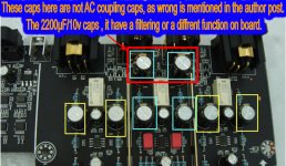
The marked caps on this picture are not AC coupling caps, but it have a different function on board. I did not yet figured out which function it may be... Their minus pole is tied to GND.
The marked caps on this picture are not AC coupling caps, but it have a different function on board. I did not yet figured out which function it may be... Their minus pole is tied to GND.
Attachments
Last edited:
The AC coupling caps (Silmic 100µ/16v) are all the rest of the marked caps in that picture, except the ones I mentioned. The small (dimensional) ones in between (220µ/16v) are filtering caps for opamps positive power rails.
Actually these AC coupling caps it should be an unpolarised type. Much better without (bypassing it), if the connected amplifier it can accept DC coupling (into 10mV offset). Before bypassing it, one should measure the DC offset before the caps, to ensure the offset is acceptable for the connected power amp/preamp.
Actually these AC coupling caps it should be an unpolarised type. Much better without (bypassing it), if the connected amplifier it can accept DC coupling (into 10mV offset). Before bypassing it, one should measure the DC offset before the caps, to ensure the offset is acceptable for the connected power amp/preamp.
The AC coupling caps (Silmic 100µ/16v) are all the rest of the marked caps in that picture, except the ones I mentioned. The small (dimensional) ones in between (220µ/16v) are filtering caps for opamps positive power rails.
Actually these AC coupling caps it should be an unpolarised type. Much better without (bypassing it), if the connected amplifier it can accept DC coupling (into 10mV offset). Before bypassing it, one should measure the DC offset before the caps, to ensure the offset is acceptable for the connected power amp/preamp.
If the preamp inputs have a cap there , a straight wire bypassing the output caps will no longer be an issue.
Yes, indeed. If the amp/preamp it is AC coupled on its inputs, then is safe to wire bypassing the AC coupling caps on Oppo outputs.
Please note about my above correction. If one wire bypass the caps wrong indicated in that picture, as AC coupling caps, then it is a catastrophic result.
Please note about my above correction. If one wire bypass the caps wrong indicated in that picture, as AC coupling caps, then it is a catastrophic result.
If the preamp inputs have a cap there , a straight wire bypassing the output caps will no longer be an issue.
The other problem of using the Oppo 205 with a preamp having AC coupling caps on its inputs is that now you have 2 coupling caps in series, which ends up increasing the low-frequency pole of the high-pass filter, potentially reducing your low-end bass response.
Yes, this is right as well.
This aspect it is a dilemma for designers: they does not know what it may be connected to the device outputs. The AC coupling is safest, but the downside is the alteration of the signal. I think the designers decision (theoretically) is right, when about a mass produced device. Another aspect is the difficulty to control the DC output offset in a production line. Well, every device it can be tested for this offset, but such operation it will increase the production costs. Also the same increasing for the costs is to design a more sophisticated output circuit, which it may make possible a more accurate control for the DC offset in a mass production line... Enough many factors... They chosen the (cost effective) easiest way.
The problem in this case, is that the AC coupling is made enough bad/cheap: a quite low value for the main coupling cap, no any bypassing for high frequencies (audio signal), and the use of not right components in this place (polarised capacitors).
I have replaced the AC coupling stage with the right approach (keeping it in place for safety reasons), but in the final, I found out that without is the best result.
At least there is quite easy to correct this AC coupling, by wire bypassing it, but one should then be sure that the further amp system it accept a DC coupling, as some +/-mV in that outputs.
Last edited:
I really can't accept that a few millivolts (even tens of millivolts) of output offset is able to trip the input section of the following preamp or amplifier. If so, then the offended design component is bad since DC removal circuits are a standard part of their design.
But Oppo could have designed a DC servo circuit on its output sections to remove any potential DC offsets. No need for output capacitors...This is standard for output sections of amplifiers to prevent DC being sent out to loudspeakers voice coils, which could potentially damage them through self-heating effects.
But Oppo could have designed a DC servo circuit on its output sections to remove any potential DC offsets. No need for output capacitors...This is standard for output sections of amplifiers to prevent DC being sent out to loudspeakers voice coils, which could potentially damage them through self-heating effects.
Yeah... They chosen cheapest way of doing...
Here is a little (design) paradox in my opinion:; using the most advanced DAC chip (assumed best performance/quality), good enough post DAC circuit design, and then using a poor AC coupling, which it downgrade the quality gain...
By the way, I should also mention here the power system for analogue stage, which it show a huge ripple at the ultra low noise regulators inputs... Well, there are many paradoxes, I can say..
We may not forget that the 95 model it had DC coupling. Since that model, Oppo adopted the AC coupling design. We can not know how they thought, and why they decided so...
Last edited:
Next time, they should offer us a bypass switch in the back of the player that's labeled AC/DC coupling. This will cure a whole bunch of problems, ofcourse assuming they use a high quality cap.
BTW, have you done any mods on the 205 audio circuitry, apart from the LPM designs you've done?
BTW, have you done any mods on the 205 audio circuitry, apart from the LPM designs you've done?
Actually, I did (designed) already a such switch/selector for optional AC/DC coupling. I will include it into the 205 mods, as for 105 too. It is an internal approach, as one may not use it very often. The boards are in production now, so very soon some pictures.
I am working right now to an extended improvement for 205 (more than LPM) for both digital and analogue sections.
Improved power system on stereo board: all Schottky rectifier diodes, better filtering caps, added pre regulators for DAC power rails, improved also these DAC power rails.
The original power approach for AvccL/R is the use of +12v rail for the two ultra low noise regulators. This is not good. It load quite much this +12v rail used mainly for opamps, it increase the heat generation, and most important the datasheet for ADM7151 (used in this case) it recommend a much lower input voltage for the regulator device, for best noise level. Well, I decided to use the second AC 6v from toroid (designated to the multi-channel DAC), only for these Avcc regulators. I do not need or use multi-channel section. I plan also to use a R core transformer instead of the original toroid, better voltage customised, to minimise the heat dissipation.
I intend to implement my fully balanced output module, as unifying the DAC channels for RCA/XLR to feed this module so.
Improved even more the headphone stage, which is already a very good design, with far better performances/quality than the rest of the device outputs.
And finally, adding the mentioned selector for convenient switching AC/DC coupling on outputs.
Implementing the clock board as well, for digital stage and DAC chip.
I hope to finish soon this enough extended work... Pictures coming also soon...
Last edited:
Some more details about the SAW oscillator used by Oppo in 205 model, to clock the audio dedicated HDMI circuit.
The SAW oscillator it output differential. The balanced clock signal is then converted to unbalanced by a supplemental component/chip, before reaching the clock input pin of the processor. Both the SAW oscillator and the balanced to unbalanced converter are powered from the digital main 3,3v. rail The power pins of these components are decoupled by double caps.
The SAW oscillator is only 10mm far from the small SMPS, which it power the Silicone Image processor.
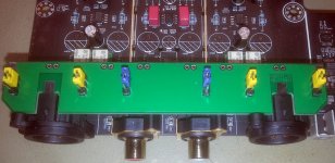
This is my solution for the AC/DC coupling selector. It fit for both 205 as 105 models. Here in picture, it is not yet connected to the output caps.
Oppo could very easy (and simple) implement a such selector into the stereo board design, giving the option to the interested user to chose the output type, for his particular configuration.
Oppo could very easy (and simple) implement a such selector into the stereo board design, giving the option to the interested user to chose the output type, for his particular configuration.
Attachments
Last edited:
- Home
- Source & Line
- Digital Source
- Oppo new UDP series players - 203/205 - Discussions, upgrades, modifications