What has to be watched is that the feedback resistor has an effect on the frequency response.http://www.ti.com/lit/ds/symlink/lme49713.pdf
no one read the data sheet - the very 1st post basic premise is wrong
the 1794 has a -6.2 mA DC bias on both outputs - biasing the I/V op amp outputs into Class A
If the op amp U1 swings 21ma pp, how the -6.2ma are enough to keep it in class A?
Dont forget that U1 has to feed R4 (570ohm) plus the dac output current.
Think before you say someone is wrong.

smms73, seeing your so handy at running sim's, could you do me a favour and run the sim on this, circuit.
Hi georgehifi,
I dont really have the time, but if you download the ltspice and create the circuit, then send it to me, i will run some simulations for you.
LTspice is a very powerfull tool and is very intuitive to create the circuit.
Nice one, jcx.
The DAC output swings 7.8 mA Pk-Pk, therefore the DAC output swings from -2.3mA to -10.1mA, i.e, the swing never crosses zero. The I/V opamp has its non-inverting input grounded. Since the current driving the inverting input never crosses zero, the opamp output never crosses zero. It never drives less than 2.3mA through Rf to maintain the voltage at the inverting input the same as the voltage at the grounded non-inverting input. Therefore it is always biassed into class A.
The fact that R4 on the output of U2 is grounded via R6 simply means that U2 is driven further into class A because it has to supply current through these 2 in addition to maintaining the net current at its inverting input at zero via its own Rf. A slightly more complicated situation pertains in regard to R3 and R5.
You guys must be reading a different datasheet, because U1 doesn't drive R4, and there's no 570R resistor.
The people at TI are no fools. Anyone who thinks they can be easily outdone might be a fool though.
I had a little think, someone is wrong.
If the op amp U1 swings 21ma pp, how the -6.2ma are enough to keep it in class A?
Dont forget that U1 has to feed R4 (570ohm) plus the dac output current
The DAC output swings 7.8 mA Pk-Pk, therefore the DAC output swings from -2.3mA to -10.1mA, i.e, the swing never crosses zero. The I/V opamp has its non-inverting input grounded. Since the current driving the inverting input never crosses zero, the opamp output never crosses zero. It never drives less than 2.3mA through Rf to maintain the voltage at the inverting input the same as the voltage at the grounded non-inverting input. Therefore it is always biassed into class A.
The fact that R4 on the output of U2 is grounded via R6 simply means that U2 is driven further into class A because it has to supply current through these 2 in addition to maintaining the net current at its inverting input at zero via its own Rf. A slightly more complicated situation pertains in regard to R3 and R5.
You guys must be reading a different datasheet, because U1 doesn't drive R4, and there's no 570R resistor.
The people at TI are no fools. Anyone who thinks they can be easily outdone might be a fool though.
I had a little think, someone is wrong.
Attachments
Nice one, jcx.
The DAC output swings 7.8 mA Pk-Pk, therefore the DAC output swings from -2.3mA to -10.1mA, i.e, the swing never crosses zero. The I/V opamp has its non-inverting input grounded. Since the current driving the inverting input never crosses zero, the opamp output never crosses zero. It never drives less than 2.3mA through Rf to maintain the voltage at the inverting input the same as the voltage at the grounded non-inverting input. Therefore it is always biassed into class A.
The fact that R4 on the output of U2 is grounded via R6 simply means that U2 is driven further into class A because it has to supply current through these 2 in addition to maintaining the net current at its inverting input at zero via its own Rf. A slightly more complicated situation pertains in regard to R3 and R5.
You guys must be reading a different datasheet, because U1 doesn't drive R4, and there's no 570R resistor.
The people at TI are no fools. Anyone who thinks they can be easily outdone might be a fool though.
I had a little think, someone is wrong.
Ok i admit, i´m only human... and i make mistakes, lots of them.

But i try to be polite.
I have take a look to the simulation again,
U2 are working in class a for shure swings between 19ma and 4.33ma
U1 is swing between 22ma and 1ma
U3 swings to -12ma to +1ma and this make it work in class b not in class a.
At 5ma pk to pk all of them work in class A.
I will try to change some resistor values to see if i can make this better.
One way or another i still think buffers are better.
Maybe i´m really a fool try to make things better , nobody can for sure.
Last edited:
Something is wrong with your sim if U1 swings to 1mA. This would mean U3 is sourcing 1.3mA of current thru R5, R3 and Rf of U1 to keep pin 2 of U1 at ground potential, and you said U3 swings -12mA to +1mA. Since you quote 4.33mA for U2, I presume +1mA is not an approximation.
You should be doing this kind of sanity checking yourself.
You should be doing this kind of sanity checking yourself.
Something is wrong with your sim if U1 swings to 1mA. This would mean U3 is sourcing 1.3mA of current thru R5, R3 and Rf of U1 to keep pin 2 of U1 at ground potential, and you said U3 swings -12mA to +1mA. Since you quote 4.33mA for U2, I presume +1mA is not an approximation.
You should be doing this kind of sanity checking yourself.
The problem is that the current imbalance caused by the voltage divider r5 r6 is not enough to put u3 in class A.
To do that you have to double r4 r5. Vout will be half 1 Vrms. And the noise increase
The resistance numbers are from the pict from post#1.
Please take a better look to the circuit. And remember that people sometimes do mistakes and that don't make them fools but only humans. Peace
Something is wrong with your sim if U1 swings to 1mA. This would mean U3 is sourcing 1.3mA of current thru R5, R3 and Rf of U1 to keep pin 2 of U1 at ground potential, and you said U3 swings -12mA to +1mA. Since you quote 4.33mA for U2, I presume +1mA is not an approximation.
You should be doing this kind of sanity checking yourself.
Instead of criticizing other people's work, why don't you get off your @ss and do a simulation yourself and then show your results? I'm sick and tired of people on this message board taking pot shots at what other people are doing without lifting a finger themselves.
I have tried to simulate the TI recommended circuit in Tina, but the software limitations prevent me from creating a good model of the DAC. Either that, or I'm just not talented enough to do it.
Last edited:
....You should be doing this kind of sanity checking yourself.
I must say, I don't feel that such chiding is at all helpful. This is intended as a hobbyist website, not a professional publication resource. Most of us have day jobs (many of which are in engineering, by the way) and have other demands on our time which limit the degree to which we are always able to "sanity check" every technical posting while participating in collaborative exchange.
We have all made the occasional technical oversight, and anyone who may believe they have never done so simply is either wrong or hasn't contributed very much that's creative or innovative. I don't wish to see interesting and creative contributions stifled by concerns of being chided for the occasional technical oversite. I suggest, that the sanity check on DIY contributions, simply due to it's avocational nature, would mostly come from fellow DIY contributors. So, sanity check all you wish, that is constructive. A smug attitude, however, is not constructive.
Last edited:
So, I have two designs for an IV converter. One has an input impedance of 3.5 ohms and THD (@1kHz) of 0.00057%. The other has an input impedance of 15 ohms and THD of 0.000058%. For both simulations, I use a current source set to 8mA in parallel with a 2kohm resistor to simulate the output impedance of the PCM1794a. Given that this DAC is designed to work into a virtual ground, would it be better to choose the one with lower input impedance in spite of the 10x higher distortion, or should I go with the one with the lower THD anyway? The noise for both is basically the same. Both have frequency response down to 1Hz at least. I should add that the one with the 3.5 ohm input impedance is made from discrete parts, so that in real life it's likely to be worse (possibly much worse) than in simulation, whereas the one with the 15 ohm input impedance is made from chips that are more likely to be closer to the sim in real life.
dirk
would you be able to post the schematics and FFT graphs?
I have been working on improving the pcm1794a by replacing the OpAmps on it. I had a thread going, looking at different op-amp combinations at the IV and gain stage of the pcm1794. My problem was that I was a noob in my LT simulation and you guys in this thread (and also another thread that is going on right now) have helped me run a proper sim.
I got some really decent results using the ADA4627 at the IV and ADA4637 and from the top of my head i think the FFT at 10kHz showed a 0.000015% THD.... I will post a screen of it later when I get home.
Anyways the ADA4627/37 combo was an improvement over the datasheet IV and gain stage.
Also I have been considering a current feedback op-amp athe IV stage but I need to know the output impedance of the PCM1794a. I have read conflicting opinions weather or not you need to know the output impedance of the DAC. Some posts have difinatively said that you are doing it wrong if you are looking at the output impedance of the PCM1794a.
How did you arrive at 2kOhm output impedance and 8ma current sourse simulation of the PCM1794 dac?
Thanks
Well, my ideas are a little radical so I'm a bit shy about posting. I've posted them elsewhere before so they are nothing really new. My solution looks nothing like the TI schematic. I use an input transformer, for example.
Some folks think that lowest distortion is not the holy grail of good sound, but I don't know myself. Your results are really good though. Everyone does what makes sense to them. In my limited knowledge, I've come up with what makes sense to me, but it boils down to two different schematics.
Well, the data sheet shows max of 7.8mA output for the DAC, so I rounded up to 8. Someone else in another discussion suggested that the real output impedance of the DAC is around 2k ohms (in parallel with a small capacitor also), so that's where I got that. Current sources are usually high impedance, but this is the digital world, where strange things can happen.
Joachim Gerhard shared this web page about IV converters:
http://www.by-rutgers.nl/IV-converter.html
The author comes to the conclusion that a really fast opamp is the best IV converter.
Last edited:
Thanks for that explanation!!!!
Very nice article! I will read it more thoroughly when I get the chance.
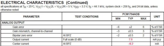
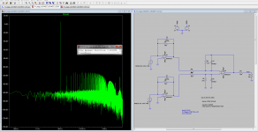
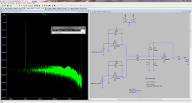
Here are my simulations..... my figures arent as impressive as i thought lol. Well two of the graphs are at 10kHz
Very nice article! I will read it more thoroughly when I get the chance.
Here are my simulations..... my figures arent as impressive as i thought lol. Well two of the graphs are at 10kHz
Attachments

OK, I had a brainstorm last night. I have a new idea (for me at least). Using the TI schematic as a template, we use current feedback opamps for the IV stages in place of the NE5534, and we use either an instrumentation amplifier or a balanced line receiver chip in place of the output opamp. Current feedback opamps have a current sensing (or responsive) input on the - pin. So, all we need to do is substitute one of these directly. The opamp arrangement TI used for the output is wrong in my opinion because it does not have balanced inputs. The inputs to that opamp are not equal impedance to ground. So, to fix that, we use an instrumentation opamp or a balanced line receiver opamp, both of which have very high CMRR and balanced inputs with single ended outputs.
So, I'm not quite awake yet which means I have not developed this idea further. I need to search the opamp catalogs for a low distortion, low noise current feedback opamp, and also select the instrumentation opamp that would perform well here.
Oh, and good morning!
So, I'm not quite awake yet which means I have not developed this idea further. I need to search the opamp catalogs for a low distortion, low noise current feedback opamp, and also select the instrumentation opamp that would perform well here.
Oh, and good morning!
I need to search the opamp catalogs for a low distortion, low noise current feedback opamp...
Joachim already mentioned the LME49713 earlier in the thread. I've built a headphone amp around this op-amp and really like it!
- Status
- This old topic is closed. If you want to reopen this topic, contact a moderator using the "Report Post" button.
- Home
- Source & Line
- Digital Source
- The pcm1794a datasheet I/V converter and how to improve it.