What a minute... isn't styrofoam slightly conductive, which would be why it is used to store chips until they're soldered? You must be getting strange results running that board with its pins and bottom conductors touching foam.forgive the 'informal construction' (lol)
Styrofoam has a very high surface resistance and you can destroy a chip pushing it into styrofoam from static buildup. Look for the black or pink foam/plastic for it to be conductive. Don't store Li cells in the pink or black foam or they will be dead. Using it this way should be fine.
Very interesting consideration, but I would say SPDIF input and USB input are fundamentally different, and should not be combined in a minimalist project.
I guess I was not clear that the combo was not a suggestion for this project. If you read through what the fifo does it is similar to what async usb is doing, in that the clock is fixed and at the dac end. The fifo acts as a dynamic buffer that allows a small difference between input and output frequencies. The output clocks could be the same clocks that the USB interface uses.
But that is not for Borge's project.
Nice! I'm working on a "formal construction" these days. The AB-1.12 board already has the ES9023 swapped out and the PCM5102 swapped in. I'm working on including the regulator by Demain and Oneoclock. In addition it will have footprints (but no PSU/IVC) for ES9012/18. It will also have an SPDIF output and improved front/back plates.
This will be a naked board (at least to begin with). That means you'll have to recycle the module and box from an AB-1.1 kit.
I'd like your input on:
- The purpose of the diode in the regulator and wheter a generic 1N4148-ish SMD can replace it.
- Pinout for external I2S interface, its driver / flip-flop and the direction of MCLK on such a thing.
Have a nice weekend!
Børge
What a minute... isn't styrofoam slightly conductive, which would be why it is used to store chips until they're soldered? You must be getting strange results running that board with its pins and bottom conductors touching foam.
I am getting one quirk: sometimes I hear skipping or some kind of data artifact; almost like analog tape saturation. I'm using older factory shipped firmware and standard linux using 16/44.1 (nothing higher; still using pulse audio). but I don't think its anything to do with the circuit. I probably need to upgrade firmware on the usb audio widget.
my longer range plans are to have the small dac on a board and also 2 gangs of spdif switch - as part of a larger preamp system. I'm thinking of using the wm8804/5 as the i2s decoder and this ti chip for the dac. the main purpose is to have 2 spdif switchable outputs, independantly, and also be able to feed one into a 'courtesy dac' (this dac chip added just because its cheap and easy and some users may find it useful).
once my wm8804 is built up, I'll move the 'foam board' (lol) to another box. for now, though, this was a super easy way for me to test the TI chip by having a convenient i2s there for me to splice into.
next test is to remove the system clock and have the TI chip derive it locally. that sounds more exciting to me; I like being able to run 1 less high speed data line!
removed the foam and moved the DAC chip over to an spdif receiver, for more testing:
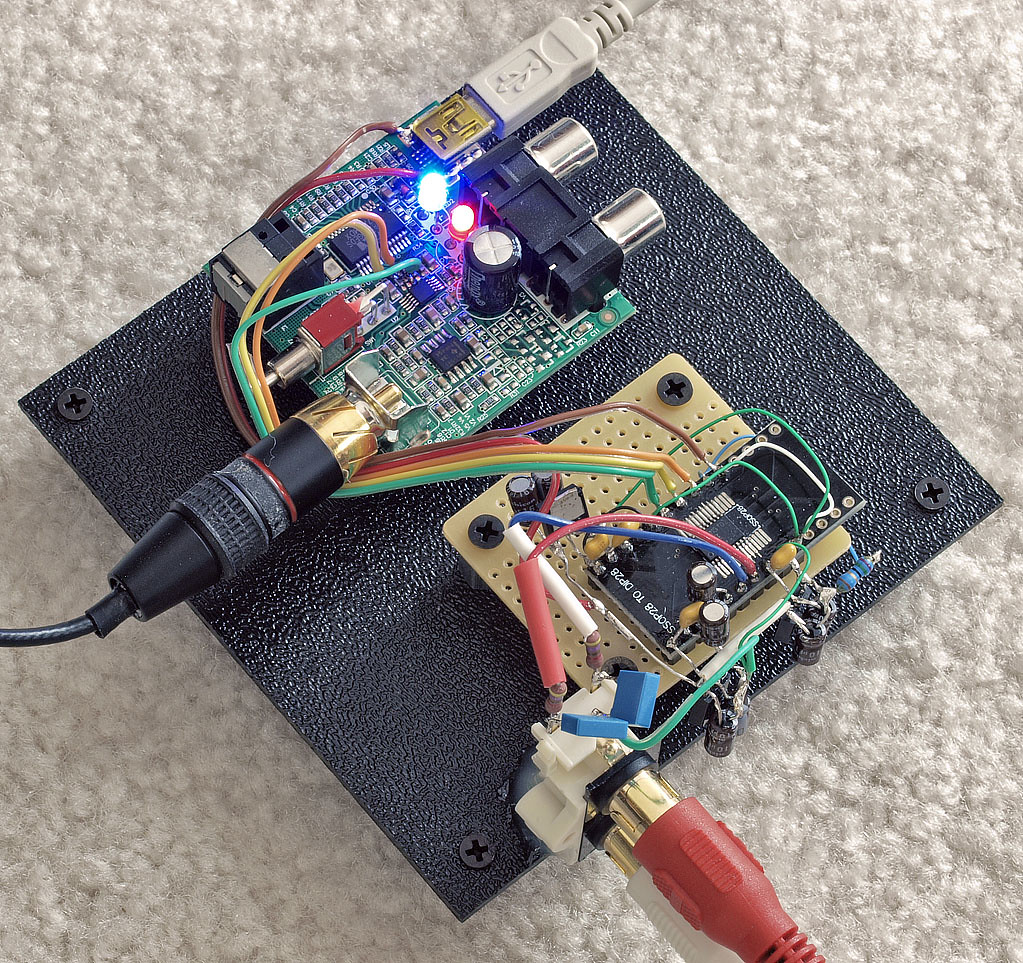
yes, I'm cheating - I'm using a $30 fiio d3 dac, out of its case, and tapping its i2s lines. (not easy to do with fat ribbon cable. I know, its my own fault, lol).
I really like this dac chip.
and I love the fact that it can run on 3wire i2s.
dump that ESS stuff and go PCM! the TI is much more DIY friendly (I was told that to buy the ESS, its min order of 25 units and is only sold via 'authorized distributors' which does not sound reassuring, to me).
I like the idea that you've designed a USB module that plugs in to an analog board. For one thing, I would like to make a balanced output analog board without necessarily messing with the USB again.This will be a naked board (at least to begin with). That means you'll have to recycle the module and box from an AB-1.1 kit.
However, I'd like to suggest that maybe you should find a way to connect the boards without having the USB module eat up a bunch of blank space on the analog board. In terms of PCB costs, this blank space represents an extra charge for most methods of fabrication. Some smaller shops charge by the square inch, and this means you pay extra. Other shops do not specifically charge by size, but they cannot fit as many boards on a panel when the boards are bigger, so it still ends up costing more.
Seems like if you swapped the back panel jacks so that the RIGHT and LEFT were on the left side and with the USB jack on the right, then your analog board could be a much smaller rectangle that only fills about half the inside of the case. The USB module would then fit on its own.
I realize that this introduces a huge problem of how to connect the two boards. Would it be better to have separate ribbon cables for LCD, UART, power, GPIO, and then special cables for I2C?
Sorry for suggesting such a drastic change, but I always find it awkward when one PCB installs over another, especially if there is nothing but blank space below.
Similar, but still fundamentally different. Although it is possible to fix the clock at the DAC end of a FIFO, it is not possible to send rate control message back through SPDIF to the media source. With USB, there is a UAC protocol that passes the rate control back through USB, the driver, and to the audio software.If you read through what the fifo does it is similar to what async usb is doing, in that the clock is fixed and at the dac end. The fifo acts as a dynamic buffer that allows a small difference between input and output frequencies. The output clocks could be the same clocks that the USB interface uses.
But, I understand that you're talking about a related design and not Børge's.
I am getting one quirk: sometimes I hear skipping or some kind of data artifact; almost like analog tape saturation.
darn it. update: it was my cd rip! doh! either a bad recording or a bad rip to flac. false alarm. carry on
")
Nice! I'm working on a "formal construction" these days. The AB-1.12 board already has the ES9023 swapped out and the PCM5102 swapped in. I'm working on including the regulator by Demain and Oneoclock. In addition it will have footprints (but no PSU/IVC) for ES9012/18. It will also have an SPDIF output and improved front/back plates.
This will be a naked board (at least to begin with). That means you'll have to recycle the module and box from an AB-1.1 kit.
that sounds good. spdif-out was one thing I wanted to add and I'm in the process of hacking a spare wm8804 into this for simple i2s->spdif conversion.
if you have room, dual output (concurrent) of toslink and coax would be a nice flexible option.
I'd like your input on:
- The purpose of the diode in the regulator and wheter a generic 1N4148-ish SMD can replace it.
- Pinout for external I2S interface, its driver / flip-flop and the direction of MCLK on such a thing.
diode? which diode? (sorry if I was not following the 100+ page thread all the way).
pinout for i2s might having .1 spacing, IDC friendly rows and alternating grounds and signal? just a guess. include power and ground on there so that the connector is 'complete'.
maybe put the 'optional' mclock toward the end. how about missing 2 pins (as sort of a key) and then putting that optional clock on one pin and a gnd on the other. that way you could run a lesser-pinned cable and ignore the last 2 pins if you don't need that clock. the gap would allow (maybe) the 'abbreviated' IDC connector for those that don't need the clock.
I have not looked too closely at the power supply schematics in this thread, but a diode in a regulator circuit is probably being used for a very specific voltage drop. You might need a Zener diode with a particular voltage drop. On the one hand, whatever diode is called for in the original circuit is probably available in an SMD package. Substitution is not necessary to get an SMD package, so I would avoid substitution unless someone carefully looks at the consequences of changing the diode.input on:
- The purpose of the diode in the regulator and wheter a generic 1N4148-ish SMD can replace it.
No point in fabricating a special regulator circuit if changes to the BoM renders its performance worse than a standard regulator.
Diode in regulator circuit
I assume the diode is to protect against reverse Vbe on the transistor and can be a generic 1N4148.
Ian
I assume the diode is to protect against reverse Vbe on the transistor and can be a generic 1N4148.
Ian
I'd like your input on:
- The purpose of the diode in the regulator and wheter a generic 1N4148-ish SMD can replace it.
I assume the diode is to protect against reverse Vbe on the transistor and can be a generic 1N4148.
Ian
I'd like your input on:
- The purpose of the diode in the regulator and wheter a generic 1N4148-ish SMD can replace it.
Bingo-
The diode is to prevent reverse current from the base of Q1, which can degrade the noise performance of Q1. Its a precaution that is unlikely to be necessary in this circuit but almost free. A 1n4148/1n914 would work fine.
Assuming that there was a particular reason to specify the 1N914 in the original schematic, how about the MMSD914T1G? That's a readily available part that I've used in other USB designs.A 1n4148/1n914 would work fine.
Assuming that there was a particular reason to specify the 1N914 in the original schematic, how about the MMSD914T1G? That's a readily available part that I've used in other USB designs.
It would certainly work. The 1n914 and 1n4148 seem to have the same die inside. This probably also has the same die. Should be about 5 cents.
mmmh, what about a small plug-in board to allow for different pinouts / I2S signal levels?- Pinout for external I2S interface, its driver / flip-flop and the direction of MCLK on such a thing.
At least in my case, MCLK should come from the widget/AB to the DAC.
I updated the regulator circuit to quell the angry tl431. Here is a link to the updated info (rather than crossposting) http://www.diyaudio.com/forums/digital-line-level/192465-asynchronous-i2s-fifo-project-ultimate-weapon-fight-jitter-25.html#post2893111 . I compensated the device to prevent it oscillating. The actual device doesn't seem to have this issue and the three pin version I use doesn't have the comp pin anyway. The curves look more like what I see with the actual circuit.
Thanks guys!
It would certainly work. The 1n914 and 1n4148 seem to have the same die inside. This probably also has the same die. Should be about 5 cents.
USB5102
I neglected to post the results of Alex's mod for allow filter switching on the PCM5102.
His new firmware and WidgetControl.py works fine with my USB5012 board. The filter selection is persistent between power cycles. I can't hear the difference between filters but that is my hearing not the filters fault.
We now have our first hardware specific control line and have the first steps toward DAC configuration via I2C lines.
There are still a few of the USB5102 kits left if anyone is interested.
George
Börge.
When do you expect the AB-1.2 be available? Can it be bought as a replacement in box to replace the AB-1.1 board? The MCU board will fit in just fine? I know, a lot of components will be thrown away but it is now as it is so far. In what positions are you planning for external PSU's optionally to be added as replacements for the built in ones? So... To be able to NOT changing the whole AB board the need is to move the DAC to somekind of piggyback board - is there a problem doing this? Money not an obstacle until you reveal your price ...
Brgds
When do you expect the AB-1.2 be available? Can it be bought as a replacement in box to replace the AB-1.1 board? The MCU board will fit in just fine? I know, a lot of components will be thrown away but it is now as it is so far. In what positions are you planning for external PSU's optionally to be added as replacements for the built in ones? So... To be able to NOT changing the whole AB board the need is to move the DAC to somekind of piggyback board - is there a problem doing this? Money not an obstacle until you reveal your price
...Brgds
- Home
- Source & Line
- Digital Source
- Open-source USB interface: Audio Widget