Extend the ground plane under the differential pair. Look for a better connector for the signals, something along the lines of this: http://www.samtec.com/documents/webfiles/pdf/QSH.PDF which is probably serious overkill. I would copy HDMI layout practices, essentially 100 Ohm diff pair for the I/V stage, but keep in mind that the virtual 0 Ohm current will become 100 Ohms (or something) at the frequency increases.
This is where an airplane board setup to have the I/V conversion as close to the pins on the chip as possible can really help. I would also look at a good current feedback opamp at that node to get the necessary power bandwidth to handle the image (typically starting at 1 MHz and still strong at 5 MHz). If it cannot handle it you will get IM and other junk. Every time a current bit switches there will be a transient. That is the biggest challenge to getting good linear performance.
This is where an airplane board setup to have the I/V conversion as close to the pins on the chip as possible can really help. I would also look at a good current feedback opamp at that node to get the necessary power bandwidth to handle the image (typically starting at 1 MHz and still strong at 5 MHz). If it cannot handle it you will get IM and other junk. Every time a current bit switches there will be a transient. That is the biggest challenge to getting good linear performance.
Many people seem to be happy with such arrangements... here is an example of a quite popular off board I/V stage: http://www.diyaudio.com/forums/digi...-sen-evolution-minimalistic-iv-converter.html
I had planned to place the I/V stage very close to the connector on my I/V board, so at least my antenna would be tuned for fairly high frequencies...")
I had planned to place the I/V stage very close to the connector on my I/V board, so at least my antenna would be tuned for fairly high frequencies...
Sorry I wasn't clear enough. Read up on how to design an -antenna- and do the opposite.
Following radio design rules is very wise in audio.
Børge
Now it make complete sense. Dipoles are fun.
Sorry guys, but I don't see it. 
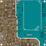
The gnd plane on solder layer (brown polygon http://www.diyaudio.com/forums/digi...b-interface-audio-widget-217.html#post3444877) is unbroken all the way from DAC chip to connector and Iout+/Iout- are routed closely together from chip to connector - where is the dipole antenna?
The gnd plane on solder layer (brown polygon http://www.diyaudio.com/forums/digi...b-interface-audio-widget-217.html#post3444877) is unbroken all the way from DAC chip to connector and Iout+/Iout- are routed closely together from chip to connector - where is the dipole antenna?
Don't worry, I am just trying to make sure I have not overlooked something obvious.
I actually once had a gain-clone amp (not my own layout), which picked up mexican radio - pretty freaky in the beginning.
National's stuff seems to do that. Back in the late 70's they had a op amp for MM cartridges that picked up any taxi near by. A few clubs downtown had this problem with their DJ mixers.
Sorry guys, but I don't see it.
The gnd plane on solder layer (brown polygon http://www.diyaudio.com/forums/digi...b-interface-audio-widget-217.html#post3444877) is unbroken all the way from DAC chip to connector and Iout+/Iout- are routed closely together from chip to connector - where is the dipole antenna?
It can be hard to see details on an image like this, especially when you can't be sure of what you can't see. You also do have what seems to be a ground adjacent to one of the traces. If its too close it could unbalance the network, otherwise it seems pretty good.
I have made a few changes: ADC connector added, correct SPI pins used, 3.3 V regulators swapped and better clearing of the current out traces.
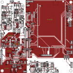
The polygons on component side are actually psu - is that bad approach in practice? One of the few things I remember from high speed subjects at university was the importance of short signal path for supplies&gnd, as well as the coolness of using the layers to make ultrafast plate capacitors in the pico range...
The first image show gnd layer - brown is AGND and cyan is DGND. Second image show the signal traces and small sections of supplies. Any comments are welcome.
You also do have what seems to be a ground adjacent to one of the traces. If its too close it could unbalance the network, otherwise it seems pretty good.
The polygons on component side are actually psu - is that bad approach in practice? One of the few things I remember from high speed subjects at university was the importance of short signal path for supplies&gnd, as well as the coolness of using the layers to make ultrafast plate capacitors in the pico range...
The first image show gnd layer - brown is AGND and cyan is DGND. Second image show the signal traces and small sections of supplies. Any comments are welcome.
Attachments
The Linux Kernel patch created for the CM6631 and the Via chip also got the Audio Widget working without the Linux hack. I posted the patches here http://www.diyaudio.com/forums/pc-based/93315-linux-audio-way-go-212.html#post3465008 for those ready to build kernel modules. Otherwise if you can get a 3.9 Kernel the patch is already in it (or so I hear).
It looks like you have done an excellent job of pulling it together. I probably would have given up and gone to a 4 layer PCB but I get lazy.
Regarding the ADC connector, I have taken the master clock directly from the isolator, so it is the same ~22MHz (of course with a small delay) used for the DAC master clock. Is that the most optimal clock for the ADC?
I'd love to see Google add native support for USB Audio Class 2.0 drivers in Android. Then, using my Android phone or tablet, I could play high res files. It would also be great if a desktop version of Android were developed and we could build HTPCs running Android.
If you'd also like USB audio support in Android, go here:
https://code.google.com/p/android/i...r Summary Stars&groupby=&sort=-stars&id=24614
and vote!
Be sure to click on the star at the bottom of the page to register your vote.
If you'd also like USB audio support in Android, go here:
https://code.google.com/p/android/i...r Summary Stars&groupby=&sort=-stars&id=24614
and vote!
Be sure to click on the star at the bottom of the page to register your vote.
Last edited:
I believe the latest Samsung devices (Note2 Tab ??) do support USB audio. I'll test that theory soon.
Is there native USB audio support on Android?
That's what I want.
- Home
- Source & Line
- Digital Source
- Open-source USB interface: Audio Widget