Timing looks good, also minus is full and plus has a value (L+R being the same), LE looks good as well, maybe it would be even better if the unused bits get suppressed. Can you identify the content of the data lines? The analyzer should be able to display DEC values. Maybe compare with the data that comes out of the DIR9001 so that you can see if MSB is handled correctly?
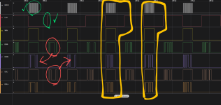
I marked red where data gets moved around. Green shows the timing: only the yellow chunks get converted. Does that correspondent with John's explanations?
I marked red where data gets moved around. Green shows the timing: only the yellow chunks get converted. Does that correspondent with John's explanations?
Attachments
Last edited:
I dont even knew there were unused bits !!!
I am not very pratical with this sofware , will try to find out for the decimal values
I will try to spot the data out of the dir9001 and bring them to the capture
the software has three analyser , Async Serial / I2C / SPI
.
I am not very pratical with this sofware , will try to find out for the decimal values
I will try to spot the data out of the dir9001 and bring them to the capture
the software has three analyser , Async Serial / I2C / SPI
.
Last edited:
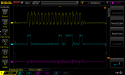
As I said: you have identical data in R and L, so it's impossible what get's copied to where - please play zero in one channel so that you can identify the content. Here is an example of input to my TDA1541A in simultaneous mode (one channel shown). You can see MSB is high. Purple is LE, yellow is BCK.
Attachments
It seems MSB gets copied into DOL+, LSB into DOL- in the first picture, and the right channel is empty. In the second picture MSB moves into DOR+, LSB into DOR- and left channel is empty.
Is that how it's supposed to work...? Please compare with Johns explanation. I thought if MSB of channel X is high the data should be copied to DOX+, else to DOX-
Is that how it's supposed to work...? Please compare with Johns explanation. I thought if MSB of channel X is high the data should be copied to DOX+, else to DOX-
Last edited:
It's a quite complicated project, so without understanding it trouble shooting will be impossible. That said it's not sooo difficult to understand. I recommend to play around with the simulator and build the glue logic online so that we can discuss it here. As an example here is my circuit from that project.
Last edited:
")
I found that other than me and John the only one who makes an left justifed converter for this set up is JOSI1 in 2018 but strangely he never report if it
worked or not , he was the one who found an error in the first converter version , unfortunately he's off forum from early 2022
from post 6200 some were dicussing about what jpk73 is talking about , with no real results or good understanding for us all
.
worked or not , he was the one who found an error in the first converter version , unfortunately he's off forum from early 2022
from post 6200 some were dicussing about what jpk73 is talking about , with no real results or good understanding for us all
.
Last edited:
Thanks for the hint! In #6205 and #6226 John explains how it's intended to work. MSB and all format related issues should be solved by his glue logic: he uses MSB to switch between the two DACs. The data each DAC receives must be COB as he uses simultaneous mode. So I think he got it right.
What is the latest version of the glue logic schematic? Did you check for all corrections done later on? I recommend to build it with the online simulator, so that we can check how it works, and than you can compare it with your circuit and do your trouble shooting. I don't see any other way to help you...!
What is the latest version of the glue logic schematic? Did you check for all corrections done later on? I recommend to build it with the online simulator, so that we can check how it works, and than you can compare it with your circuit and do your trouble shooting. I don't see any other way to help you...!
The last schematic he posted was in #8110: did you compare it to the earlier one? As i2s is only one cycle different from left justified it should be possible to verify that your version is correct. You can also have a look at PCM63 data sheet (page 5) to understand how data is fed to the 2 DACs. Regarding the simulator: start with an easy circuit such as the "flip flop devide by 3" example, and you will see it's easy to understand.
- Home
- Source & Line
- Digital Line Level
- Building the ultimate NOS DAC using TDA1541A