sparkle said:how do You set this thing to work properly? I know that I should have 2 volts on input of the i/v and I know that it should be trimmed with VR1 but from which side do You start- from which value of the VR1. Regards
daniel

When you set the I/V stage first time, the TDA1543 is diconnected.
Trim the pot until you have 2,00 volts at the source , than you swich off the supply , and wait for discharge. Than connect the TDA to the I/V stage, power up both circuits and do the final trimming.
Re: Re: Balnced Arrangement
Reclock: first off , do you think I need 2 FF in series to do the reclock? or just one in sinchronous mode?
No inverters, no buffers? You know , it is just fiew days that the XOR buffers are working in the circuits and every time I change something in the set up is like to jump off the spring-board
And jitter is so underhand
What is the way of inverting clock? I re read your .pdf for the split LR version I admit it is interesting to me and I feel like I am close to the possibilty of making an effort like that, if you have a pcb of your work I will be interested for sure
guido said:
Two idea's for improvements:
reclock all the data with FF's: use '74 so you don't need inverters and reclock with the tentclock. You will loose jitter created by the 7310 (don't know the timingrelation between 7310 I2S out and it's clock input but it should be possible). Maybe you need to invert the clock to the 7310.
Second, obvious (coming from me
I2S streams and use one dac for left and one for right.
Greetings,
Reclock: first off , do you think I need 2 FF in series to do the reclock? or just one in sinchronous mode?
No inverters, no buffers? You know , it is just fiew days that the XOR buffers are working in the circuits and every time I change something in the set up is like to jump off the spring-board
And jitter is so underhand
What is the way of inverting clock? I re read your .pdf for the split LR version I admit it is interesting to me and I feel like I am close to the possibilty of making an effort like that, if you have a pcb of your work I will be interested for sure
Re: Re: Re: Re: The Pass D1 For Tda1543
...it is also true that the I/V stage does not amplifies current.
rfbrw said:
You are confusing the specific with the general.
...it is also true that the I/V stage does not amplifies current.
Great , but probably the buffers has to be modified too. The source follower load resistor.HBarske said:Very interesting project. Cheap, fully balanced and very compact.
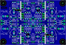
Might be an interesting match for my version of D1 output stage, which measures 80x40 millimeters (stereo, balanced, single sided board):
HI!
Mr. Billiani - thanks You made my day .
I was allways wondering how to trim the active i/v ......none of my question were answered until now. Thanks again!
regards
daniel

edit:
HBarske- I can't see that You are using volume control like in d! service manual- if so- what is the maksimum output that You get out of it?
Mr. Billiani - thanks You made my day
.I was allways wondering how to trim the active i/v ......none of my question were answered until now. Thanks again!
regards
daniel
edit:
HBarske- I can't see that You are using volume control like in d! service manual- if so- what is the maksimum output that You get out of it?
Component values certainly will have to bei modified. The values above are the original ones.Great , but probably the buffers has to be modified too. The source follower load resistor
sparkle said:HI!
Mr. Billiani - thanks You made my day
daniel
I am glad
HBarske said:Component values certainly will have to bei modified. The values above are the original ones.
As you see I considered the no-buffer option - if a preamp is used, of course- and works great before the BOSOZ.
cheers
You are not wrong if we are using for instance TDA1541 but in case of TDA1543 and TDA1545 we need something in the positive side (2V or little more for the 1543 and littl more for 1545) it is all said at few first posts of this thread. Or am I wrong now?
Also the output voltage for measuring is taken fron pin 6 and 8 of the TDA1543 and between ground. Pin 7 (Vref) stays in the air (not connected). Correct me if I made a mistake, please.
regards
daniel
Also the output voltage for measuring is taken fron pin 6 and 8 of the TDA1543 and between ground. Pin 7 (Vref) stays in the air (not connected). Correct me if I made a mistake, please.
regards
daniel
HBarske said:My suggestion refers to your idea in post #16, of course "no buffer" is an option.
I still talk of the balanced dac as in post#16 , by "no buffer" I mean the absence of the source followers in the D1 stage.
That's a good one.HBarske said:
Correct me if I am wrong:
I don't think there is much to trim - just adjust the pots until you have 0 Volts between Vref of the TDA1543 and the input of the D! output stage (no connection but ground made between them, of course).
Aaah - thank you!by "no buffer" I mean the absence of the source followers in the D1 stage
I should read the whole thread a little more concentrated I think

sparkle said:You are not wrong if we are using for instance TDA1541 but in case of TDA1543 and TDA1545 we need something in the positive side (2V or little more for the 1543 and littl more for 1545) it is all said at few first posts of this thread. Or am I wrong now?
Also the output voltage for measuring is taken fron pin 6 and 8 of the TDA1543 and between ground. Pin 7 (Vref) stays in the air (not connected). Correct me if I made a mistake, please.
regards
daniel
Daniel,
once you set the circuit as I suggested above is possible to trim the pot till the Voutput(at the source of D1) is EQUAL to Vref -as HBarske suggested. This voltage varies slightly from chip to chip and is around 2._ _volts.It seems to me a good idea.
sparkle said:Hi!
One more- did somebody tried to trim the original schematic from D1 from Mr. Pass to 2V or little more to make it suitable for our TDA1543?
regards
daniel
I modified the circuit just for it (beside the gain-drain resistor)since the original one didn't reach 2 volts.This one can trim over 4.
Oh boy!
I have sommething to learn .
.
O.k. I got it now.
Mr. Billiani I got the way to trim and with the other post in this thread it would be like walking on a ground to trim it. Sorry for my easy questions if they did bother You but I have really much to learn and the forum is the place where I can ask.
Thanks
will try that I/V and look forward for a new posts on this thread
regards
daniel
I have sommething to learn
.O.k. I got it now.
Mr. Billiani I got the way to trim and with the other post in this thread it would be like walking on a ground to trim it. Sorry for my easy questions if they did bother You but I have really much to learn and the forum is the place where I can ask.
Thanks
will try that I/V and look forward for a new posts on this thread
regards
daniel
nar said:So guys has someone succeeded in adapting the circuit to the 1545 ?
Should sound nice ....
The only big difference between the implementation around the output sections of these DACs is the different full-scale current, which is lower for the 1545.
Increasing the 680R to compensate the voltage difference should be just fine.
Cheers
Andrea
Re: Re: Re: Balnced Arrangement
Back to digital.
One FF should do it, i think but you need to look carefull at the timing between the master clock in and the output of the 7310 I2S. It should not happen that the FF inputs are changing state at the same time as the FF is clocking the data. So you might need an inverter in the clock towards 7310.
If you use '74 FF it will do the inversion for you: it has normal and inverted output! But then you need two of them for the three i2s lines. Or use one inverter chip and e.g. '174 FF.
About the splitting, there are two guys posting that they are doing this with bigger prog. logic. Only one chip then, but many small smd pens.
PCB can be bought, but further improvements can be made to the reclocking (not to mention the DAC side of things): still need to modify the GAL so I2S-clock is also latched output and then clock the FF in the GAL with inverted 11MHz clock: jitter of '161 removed
mvg,
stefanobilliani said:
Reclock: first off , do you think I need 2 FF in series to do the reclock? or just one in sinchronous mode?
No inverters, no buffers? You know , it is just fiew days that the XOR buffers are working in the circuits and every time I change something in the set up is like to jump off the spring-board
And jitter is so underhand
What is the way of inverting clock? I re read your .pdf for the split LR version I admit it is interesting to me and I feel like I am close to the possibilty of making an effort like that, if you have a pcb of your work I will be interested for sure
Back to digital.
One FF should do it, i think but you need to look carefull at the timing between the master clock in and the output of the 7310 I2S. It should not happen that the FF inputs are changing state at the same time as the FF is clocking the data. So you might need an inverter in the clock towards 7310.
If you use '74 FF it will do the inversion for you: it has normal and inverted output! But then you need two of them for the three i2s lines. Or use one inverter chip and e.g. '174 FF.
About the splitting, there are two guys posting that they are doing this with bigger prog. logic. Only one chip then, but many small smd pens.
PCB can be bought, but further improvements can be made to the reclocking (not to mention the DAC side of things): still need to modify the GAL so I2S-clock is also latched output and then clock the FF in the GAL with inverted 11MHz clock: jitter of '161 removed
mvg,
- Status
- This old topic is closed. If you want to reopen this topic, contact a moderator using the "Report Post" button.
- Home
- Source & Line
- Digital Line Level
- The Pass D1 For Tda1543