Andypairo said:
C'mon Stefano,
don't be shy!
This topic deserves a thread of his own, so.. just post it
Cheers
Andrea
Thanks Andrea!!!!
So... it is ... here.
What can I say?
a: I didn't ask Nelson Pass for copyright problem but since the design is modified , they should not exist
") BTW Thanks Nelson!
BTW Thanks Nelson!b: leave out vref resistor
c: once set up is done , nothing changes if you change the VCC at the 1543;
d: like c , nothing changes if you decide to parallel the 1543; in this regard to obtain ,IMHO ,great results with 2 1543 in parallel is simple: great dynamics.
e: it sounds like a single TDA1543 would enjoy a bigger source resistor , but this is another matter.
f: IRF630 is used by me for comfort , and I believe IRF610 will pay better in performance.
g: cascode is not a gain stage.
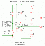
I do not know if something is missing , but guys ... take a look at the schematic , isn't it simple?
I'd say... YES!!!
Attachments
- since the simplicity of the circuit is up to you decide what is your favourite , but Yes it is compared with the single resistor at the output ...
- YES but you may want to adjust the drain resistor for gain
- I use a power supply like BOSOZ but scaled down for +/- 30 Volt
- YES but you may want to adjust the drain resistor for gain
- I use a power supply like BOSOZ but scaled down for +/- 30 Volt
Hi!
This is very nice I must say.
Few questions- You have mentioned to leave out vref resistor. I don't see that one in schematic. Also what power supply did You use for powering TDA1543 chip (voltage also please).
regards
daniel
edit: One more thing- I think that TDA1543 like to have 0V at his output and not 2V?! Am I wrong?
Wrong
edit: One more thing- I think that TDA1543 like to have 0V at his output and not 2V?! Am I wrong?
Yep you're wrong, but the TDA1541A does not like DC on its output, the TDA1543 has lots of DC on its output in most of the passive I/V DACs, anyone know how closely related these two DACs are?
Mozfet
edit: One more thing- I think that TDA1543 like to have 0V at his output and not 2V?! Am I wrong?
Yep you're wrong, but the TDA1541A does not like DC on its output, the TDA1543 has lots of DC on its output in most of the passive I/V DACs, anyone know how closely related these two DACs are?
Mozfet
Re: Re: The Pass D1 For Tda1543
I quote MR Pass from a Passlabs thread:
...
rfbrw said:
I quote MR Pass from a Passlabs thread:
Nelson Pass said:I have a current working definition of what constitutes a
gain stage - it is a stage with voltage or current gain, and I
don't count cascodes with no current gain.
...
sparkle said:Hi!
This is very nice I must say.
Few questions- You have mentioned to leave out vref resistor. I don't see that one in schematic. Also what power supply did You use for powering TDA1543 chip (voltage also please).
regards
daniel
edit: One more thing- I think that TDA1543 like to have 0V at his output and not 2V?! Am I wrong?
By "leave out the vref resistor" I meant just to let the pin 7 of 1543 disconnected.
You may use what power supply you want from 5 to 9 volts , the source pin will be stable at 2 volts ,regardless of the variations of voltage at pin 5 of tda1543.
BTW I am using 8 volts and 2 tda1543 in parallel / phase .In the sense that the dac is balanced at the moment and counts 4 dacs in total.I will post a block diagram of it soon if it is of interest.
The power supply is a discrete op amp -take a look at the Pearl ONO- followed by a current source or jfet source follower.I have an unregulated supply about 30 volts.
The discrete op amp is at 12volts . The current source eat up at least 4 volts . But i am still in making decisions about it.
For the TDA1541A you trim the source for 0 volts , and use the ORIGINAL PASSLABS circuit.
For the TDA1543 not 0volts but 2,0 or higher voltage .
I also will try soon the circuit with the 1545A.
Re: Wrong
The main difference (apart from the circuit refinement) is that the TDA1543 (and1545) use a single supply, while the TDA1541 uses a dual supply for the analog section.
Since the output section of these DACs is made of current sources/sinks it is not possible for the single supply chips to have 0V on their output (at least while working ).
Hope this clears things a little.
Cheers
Andrea
mozfet said:edit: One more thing- I think that TDA1543 like to have 0V at his output and not 2V?! Am I wrong?
Yep you're wrong, but the TDA1541A does not like DC on its output, the TDA1543 has lots of DC on its output in most of the passive I/V DACs, anyone know how closely related these two DACs are?
Mozfet
The main difference (apart from the circuit refinement) is that the TDA1543 (and1545) use a single supply, while the TDA1541 uses a dual supply for the analog section.
Since the output section of these DACs is made of current sources/sinks it is not possible for the single supply chips to have 0V on their output (at least while working
).Hope this clears things a little.
Cheers
Andrea
Bricolo said:But where's the cascode here
I don't see a cascode in your circuit, nor in Pass Labs original D1 one (the second transistor is a buffer, not a cascode)
Bricolo,
the DAC is looking for a virtual ground - the source of the mosfet .Than the signal is amplified in voltage by the mosfet that is in common gate mode .
If not cascode , than what?
stefanobilliani said:
By "leave out the vref resistor" I meant just to let the pin 7 of 1543 disconnected.
For the TDA1543 not 0volts but 2,0 or higher voltage .
I also will try soon the circuit with the 1545A.
Hello Stefano,
I hadn't noticed that...this way you switch off the internal current sources of the 1543 and feed its outputs (that now act only as current sinks if I understand right) through the Mosfet, which seems to be configured as a common gate.... the 3k3 sinks further 10mA to keep the fet well polarized and the current variations due to the DAC are reflected on the 680R resistor... very clever!
Did I get it right?
Cheers
Andrea
PS For the balanced are you still using the circuit posted some time ago?
Andypairo said:
Did I get it right?
Your description is good
thanks.NO.Andypairo said:For the balanced are you still using the circuit posted some time ago?
I think I'll post tonight the arrangement, based on XOR gates that acts as buffers and inverters.
YESSSS!
Thats was the piece of the puzzle that I need to figure out. That helped a lot. I did know that this chip has dc output voltage- well I have dac at home- but don't ask me why I didn't figure it out. Maybe I'm to stupid or something - maybe it was blocked for me to get to know today. I don't know- anyway it was a great help.
I REALLY WOULD LIKE TO SEE THAT ARANGEMENT OF YOURS Mr. Bilianni. I have thought to make it ballanced this time but with a single TDA chip (not in paralel). My friend has aleph 5 and aleph 1.7 is on the way and this arangement would be so helpfull I can't tell You how much. It would save me some time of thinking and making questions on the forum.......
regards
daniel
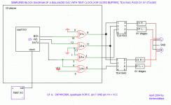
Balnced Arrangement
OK this is the actual balanced DAC arrangement .Of course it is simplified a lot in the sense that some care has to be taken for the shielded connections , the decoupling caps, ferrite beads and low noise power supplies.
Some thing can be of help BTW:
The buffers need its own PS or at list they can be attached at the DAC VCC but for the SN74HC86N the limit is 7V AND NOT 9V like the 1543.
The 1543 needs its own PS.
The buffers can be mounted close to the dacs , maybe it would be better maybe not.
The Tent clock needs its own PS of course.
The Passlabs D1 stages needs its own PS : +/- 30volts.
The I2S and cloock lines outside the player MUST be shielded .
Attachments
Thanks mr. Bilianni!
It is very similar like in the D1 d/a converter (in fact the connection is the same). One more thing- because I have allways wondered about that- You connect everything together like in those schemtaics (that is not a problem to me) and how do You set this thing to work properly? I know that I should have 2 volts on input of the i/v and I know that it should be trimmed with VR1 but from which side do You start- from which value of the VR1. Please understand, I don't want to destroy my TDA chip and really I don't know very much about them so I must ask.
I don't know if my dac would live long enough for his i/v to get trimmed.
I would appreciate if nobody would laugh at me and if somebody would help me to understand.
Regards
daniel
Re: Balnced Arrangement
Two idea's for improvements:
reclock all the data with FF's: use '74 so you don't need inverters and reclock with the tentclock. You will loose jitter created by the 7310 (don't know the timingrelation between 7310 I2S out and it's clock input but it should be possible). Maybe you need to invert the clock to the 7310.
Second, obvious (coming from me ): split left and right into two
I2S streams and use one dac for left and one for right.
Greetings,
stefanobilliani said:OK this is the actual balanced DAC arrangement .Of course it is simplified a lot in the sense that some care has to be taken for the shielded connections , the decoupling caps, ferrite beads and low noise power supplies.
Some thing can be of help BTW:
The buffers need its own PS or at list they can be attached at the DAC VCC but for the SN74HC86N the limit is 7V AND NOT 9V like the 1543.
The 1543 needs its own PS.
The buffers can be mounted close to the dacs , maybe it would be better maybe not.
The Tent clock needs its own PS of course.
The Passlabs D1 stages needs its own PS : +/- 30volts.
The I2S and cloock lines outside the player MUST be shielded .
Two idea's for improvements:
reclock all the data with FF's: use '74 so you don't need inverters and reclock with the tentclock. You will loose jitter created by the 7310 (don't know the timingrelation between 7310 I2S out and it's clock input but it should be possible). Maybe you need to invert the clock to the 7310.
Second, obvious (coming from me
): split left and right into twoI2S streams and use one dac for left and one for right.
Greetings,
- Status
- This old topic is closed. If you want to reopen this topic, contact a moderator using the "Report Post" button.
- Home
- Source & Line
- Digital Line Level
- The Pass D1 For Tda1543