Hello Ian,
Hope you are well!
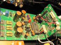
I am assisting a fellow Australian in connecting up the i2stoPCM to a TDA1541 ... I had a look at your PCB layout in post 242 and noticed the silkscreen in the manual for DCOUT/GND on TP9/TP1 appears to be back to front. He has the boards so I dont have one handy to poke at, could you confirm the polarity for the connection to the isolator board from these test points? I think TP9 should be +ve output rather than GND.
I also noticed that these connections are not mentioned in the manual, would be handy to have them mentioned if ever a new revision to the i2s to PCM converter manual is released.
Regards,
Chris
Hi Chris,
I'm not Ian but I do have this board in front of me. The TP's are just that, test points. PT9 labelled as GND. But surely, even it its mislabelled you'd read -5V instead of 5V and it would be obvious. In effect, of course all you need do is connect the 5VDC to 'DC Input' which is clearly labelled WRT polarity..
hth
Shane
Attachments
Last edited:
Hi Chris,
I'm not Ian but I do have this board in front of me. The TP's are just that, test points. PT9 labelled as GND. But surely, even it its mislabelled you'd read -5V instead of 5V and it would be obvious. In effect, of course all you need do is connect the 5VDC to 'DC Input' which is clearly labelled WRT polarity..
hth
Shane
Hi Shane,
Yep that's exactly what I suggested to him last night ... I just wanted to post so that Ian can confirm as some might not check.
It might be a handy option for you if you wanted to connect your i2stoPCM board and DualXO board to one PSU (one PSU on each side of the v2.5 isolator board). If you've got a lower noise PSU on the dualXO board now, you may find using it to power both of those boards is preferable to the 7805 that it looks like is being used off the AYA II board.
I'll be building a 2014 AYA II and probably connect it the way I've just described above myself. I have designed a dual +ve regulator board for myself that uses an adjustable LM317 to reduce voltage drop across a TPS7A4700 for isolated low noise outputs. Need to do some measurements of the noise at some point but need to DIY the tools for that yet
")
I will be using Si570 though and running the second i2s output from the Si570 to a separate DAC so that I can do some comparisons between DACs with a synchronised and low jitter data stream which is perfect for A/B comparisons!
Cheers,
Chris
Please look at this board, it can drive PCM DACs directly with XMOS chip.
I2SoverUSB - I2S over USB Audio
Here are connection circuits
http://www.jlsounds.com/uploads/Specifications.pdf
I believe they get PCM data right from USB input and not even convert it to I2S first or make conversion on a single board in the XMOS chip? Looks like better (simpler, shorter path) solution than using I2S board and then conversion board. What are your thoughts?
It might be a handy option for you if you wanted to connect your i2stoPCM board and DualXO board to one PSU (one PSU on each side of the v2.5 isolator board). If you've got a lower noise PSU on the dualXO board now, you may find using it to power both of those boards is preferable to the 7805 that it looks like is being used off the AYA II board. !
Cheers,
Chris
Hi Chris,
I'm using ISO > Dual XO > I2S to PCM in that order which then feeds the 1541A in simultaneous mode, each with separate supplies provided by separate windings on the PT secondary.
The AYA II board doesn't use 7805.. or any other three terminal reg. When you get your board you'll see exactly what I'm meaning. Very nice discrete regulators, operating without feedback and buffered for very low Zout.
As you can see, its a cut-down AYA board, so there are supplies which aren't used for CS receiver etc, which can be put to good use for clocks, PCM boards etc.
hth
Shane
Please look at this board, it can drive PCM DACs directly with XMOS chip.
I2SoverUSB - I2S over USB Audio
Here are connection circuits
http://www.jlsounds.com/uploads/Specifications.pdf
I believe they get PCM data right from USB input and not even convert it to I2S first or make conversion on a single board in the XMOS chip? Looks like better (simpler, shorter path) solution than using I2S board and then conversion board. What are your thoughts?
Any direct experience?
Any direct experience?
not yet... it is hard to compare anyway unless it is direct switch on/off which is not possible in most of the cases. so that is fight of theory only
but if i were them to design it i see no reason to make it right since that purpose was there from the beginning.
Last edited:
Hi Chris,
I'm using ISO > Dual XO > I2S to PCM in that order which then feeds the 1541A in simultaneous mode, each with separate supplies provided by separate windings on the PT secondary.
The AYA II board doesn't use 7805.. or any other three terminal reg. When you get your board you'll see exactly what I'm meaning. Very nice discrete regulators, operating without feedback and buffered for very low Zout.
As you can see, its a cut-down AYA board, so there are supplies which aren't used for CS receiver etc, which can be put to good use for clocks, PCM boards etc.
hth
Shane
Ah, I had some vague recollection of an AYA DAC with 7805 powering those digital parts of the circuit. Will build those supplies and compare them too, hopefully i will have the tools to be able to measure the complete system too by the time I have these built.
Ah, I had some vague recollection of an AYA DAC with 7805 powering those digital parts of the circuit. Will build those supplies and compare them too, hopefully i will have the tools to be able to measure the complete system too by the time I have these built.
The new regs will knock ur socks off… and I know because I have been there.
Mr. Rogic knows what he is doing, and he has it nailed down, doesn't take him a thousand revisions.
Last edited:
Please look at this board, it can drive PCM DACs directly with XMOS chip.
I2SoverUSB - I2S over USB Audio
Here are connection circuits
http://www.jlsounds.com/uploads/Specifications.pdf
I believe they get PCM data right from USB input and not even convert it to I2S first or make conversion on a single board in the XMOS chip? Looks like better (simpler, shorter path) solution than using I2S board and then conversion board. What are your thoughts?
EDIT I posted without looking at the design, they've got isol and reclocking covered. That looks like a reasonable design. I'm not a huge fan of the xpresso clocks but they aren't bad per-se. The pin headers for inputting an external clock is a bit of a red flag though ... for a high speed clock clock a pin header is not best practice design, u.fl is preferred there.
Last edited:
thank you for reply. I agree, Ian`s products are great!!! I am using AD1865 based AudioNote DAC so i am happy to avoid CS8414 and connect it via bit perfect I2S to USB. But still i see no real reason in all of this additional board if you have right converter... Just imagine, you have good master clock located right near the DAC chip and route its MCLK to the USB->PCM converter. You can program XMOS in any way and output PCM directly, it is bit perfect with buffer already so there should not be any losses. And since you are using single clock to sync both dac chip and converter there is minimal jitter. I agree we need isolator from the USB but this is that jlaudio is having with reclocking from the same external clock. Isn't is the best and shortest way for the particular purpose of the delivering data from PC to dac chip?
EDIT I posted without looking at the design, they've got isol and reclocking covered. That looks like a reasonable design. I'm not a huge fan of the xpresso clocks but they aren't bad per-se. The pin headers for inputting an external clock is a bit of a red flag though ... for a high speed clock clock a pin header is not best practice design, u.fl is preferred there.
Ah, I had some vague recollection of an AYA DAC with 7805 powering those digital parts of the circuit. Will build those supplies and compare them too, hopefully i will have the tools to be able to measure the complete system too by the time I have these built.
eh?.. you'll build 'those supplies', with respect, you don't know what your talking about.
Shane
eh?.. you'll build 'those supplies', with respect, you don't know what your talking about.
Shane
By 'those supplies' I just meant the PSUs that were intended for sections of the aya ii board I won't be using - without a better name for them. I have seen the new 2014 schematic , the 7805 reference earlier was only because I thought I had seen older aya dac boards with them. Surely thete is no harm in building, measuring and listening to so i can compare a few options and deciding what I prefer?
Chris
eh?.. you'll build 'those supplies', with respect, you don't know what your talking about.
Shane
He does actually, your just mis-interpreting him. The old pre Aya Rodjic board had 78xx regs. I've got some of h's current psu boards and they are very good.
No, Maloney..
Were talking about current AYA2… as is his current project.
BTW your 5881 regs are kinda - well, ****.
And yeah I've built them.. tried different zener refs.. all the rest but theres better.
Not so much better, but 25% is enough for most who have ears.
Love from he who builds and then listens
Were talking about current AYA2… as is his current project.
BTW your 5881 regs are kinda - well, ****.
And yeah I've built them.. tried different zener refs.. all the rest but theres better.
Not so much better, but 25% is enough for most who have ears.
Love from he who builds and then listens
Last edited:
thank you for reply. I agree, Ian`s products are great!!! I am using AD1865 based AudioNote DAC so i am happy to avoid CS8414 and connect it via bit perfect I2S to USB. But still i see no real reason in all of this additional board if you have right converter... Just imagine, you have good master clock located right near the DAC chip and route its MCLK to the USB->PCM converter. You can program XMOS in any way and output PCM directly, it is bit perfect with buffer already so there should not be any losses. And since you are using single clock to sync both dac chip and converter there is minimal jitter. I agree we need isolator from the USB but this is that jlaudio is having with reclocking from the same external clock. Isn't is the best and shortest way for the particular purpose of the delivering data from PC to dac chip?
Well I am not sure it would have any advantage over Ian's solution though it will be cheaper. The concern for me is the RFI radiated by poor connection of the clock between your DAC and the jlaudio board.
The jitter is created at the reclocking stage so the clock should electrically be as close to the reclocking circuit as it is to the DAC chip. This is where u.fl and Ian's PCB layout have advantages ... Those jlaudio layouts look like their clock traces are too narrow. Hard to say which is better. The jlaudio board is cheaper and has less parts which is appealing but the additional complexity of Ian's solution does come with some advantages.
so the only issue you see is poor external clock connector? it can be fixed easily i guess. I am talking not about particular jlaudio board but concept itself. Master clock path is shorter with jlaudio type solution comparing to all of the Ian`s extra boards so with a good connection and location should have less jitter. Thus looks like custom firmware for XMOS chip to output PCM instead of the I2S makes this solution better theoretically.
Well I am not sure it would have any advantage over Ian's solution though it will be cheaper. The concern for me is the RFI radiated by poor connection of the clock between your DAC and the jlaudio board.
The jitter is created at the reclocking stage so the clock should electrically be as close to the reclocking circuit as it is to the DAC chip. This is where u.fl and Ian's PCB layout have advantages ... Those jlaudio layouts look like their clock traces are too narrow. Hard to say which is better. The jlaudio board is cheaper and has less parts which is appealing but the additional complexity of Ian's solution does come with some advantages.
No, Maloney..
Were talking about current AYA2… as is his current project.
BTW your 5881 regs are kinda - well, ****.
And yeah I've built them.. tried different zener refs.. all the rest but theres better.
Not so much better, but 25% is enough for most who have ears.
Love from he who builds and then listens
Where did you get that chip on your shoulder?
so the only issue you see is poor external clock connector? it can be fixed easily i guess. I am talking not about particular jlaudio board but concept itself. Master clock path is shorter with jlaudio type solution comparing to all of the Ian`s extra boards so with a good connection and location should have less jitter. Thus looks like custom firmware for XMOS chip to output PCM instead of the I2S makes this solution better theoretically.
The ideal approach would be to have the PCM signal reclocked on the DAC board and have the master clock feed that reclocking circuit directly (PCM doesn't feed MCLK to the DAC) and then feed by u.fl back to the USB board isolators on the jlaudio board (or similar). There would need to be two master clocks available on the DAC board and XO selection fed from the jlaudio board to the DAC. Since no DACs have been designed like this ... IMO ... Ian's implementation is technically better at accommodating the DAC boards that are currently available. How much better? I don't know. Is it worth the extra $$? I don't know that either.
Where did you get that chip on your shoulder?
ha!
you're right.
unresolved issues.. which I guess why I spend too much time away from the populous.. but when I do venture out, it does become apparent.
No disrespect intended.. I just didnt like your 5881 regs, thats all. Completely off topic and un-warranted.
Ive just been looking at Ian's PCM board design and Im immensely impressed.
For DIY TDA1541a projects being able to drive the chip with simultaneous offset binary mode is a breakthrough.
I cant see any other USB boards that can do that but do let me know if Ive missed one.
Big thanks to Ian.
For DIY TDA1541a projects being able to drive the chip with simultaneous offset binary mode is a breakthrough.
I cant see any other USB boards that can do that but do let me know if Ive missed one.
Big thanks to Ian.
- Home
- Source & Line
- Digital Line Level
- Drive NOS AD1865/62,PCM1704/02/63,TDA1541 from FIFO: Universal I2S-PCM driver board