I did careful compare in between, the OCXO is better than Si570.
Ian
Hi,Ian very good news.
I have the OCXO master clock , but it's sitting on the best point in the Isochrone OCX unit with many BNC outputs.
Need your Any advice to feed / instead of mck on your FIFO & I2S to PCM board.
Thanks and best regards
power supply questions; clock board question
Hi all, i have finally made the decision to join the FIFO club, but i have some very basic questions.
1. Which clock board to buy?
I'm guessing the right answer to this is probably going to be: Ian's new clock board that is still under development.
... but in the meantime, i'm unsure whether the dual clock board or the Si570 would be best for me.
To provide context, I plan to use the FIFO with at least two different DACs: one of these is a commercial "Line Magnetic" Sabre-based DAC, where i plan to replace the existing XMOS based USB-I2S board with an Amanero-FIFO-isolator-clock combination.
However, the I2S from that board to the main DAC board does not appear to include an MCLK signal, as it only has 3 wires, presumably the standard I2S signals of SD, SCLK, and L/RCLK.
The other DAC will be a TDA1541A DAC, and since I will want to use Ian's I2StoPCM board, this is where I assume the MCLK signal will be important.
So any advice on which clock board would be best for my applications would be greatly appreciated. I want the best sound quality, although I cannot afford those Pulsar clocks!
2. My second question concerns the power supplies.
I understand the FIFO requires 6V 500mA, and the Si570 clock board "4-6V, 150mA". I am not sure what voltage is required by the dual clock board.
The I2StoPCM board requires 4-6V 50mA.
Although i have not read every post on this thread, i have spent a while trawling through it and have not found any information on what supplies to use (other than recommendations to use A123 batteries, which i may try in future, but i plan to start with a conventional power supply).
So, my question is: are there are recommended power supply boards for use with Ian's boards? And a very noob question: what transformer secondary voltage/current/VA would be recommended (although i expect this may weakly depend on what supply board is used...?). Also, i note Ian's regulator board for use with the Si570 clock, but when that is used, i assume i still need to supply a regulated supply to that board?
[edit: oh,. and will i need to buy any connectors to interconnect all of the above boards, or does Ian supply all that i will need?]
Thanks in advance,
richard
to feed the question above a little as I'm lost as well:
Which Fhz Crystal is needed if music is upsampled by the computer (on fly by the soft streamer or before then recorded updsampled in the library) before streaming to the I2StoPCM board then the TDA1541 ? Does the MCLK of the I2StoPcm board need a minimal MCLK speed ?
Better a NOS or a NNOS (Near NOS speed (x 2) like 96K ) with already upsampled music or a TDA1541 playing at 380 khz as its datasheet alow ?
Is there a subjective Sound Quality improvement when genuine 44 Khz or 96 Khz (most of my tunes library) is streamed (without upsampling) on a TDA1541 with a clock speed of 380 Khz ?
I'm a little lost between the concept of upsampling and the concept of interest to playing red book or 96 khz without upsampling but with oversampled speed of the hardwares.
Are the glitchs really removed by upsampling or oversampling ?
Sorry if already asked or for my missunderstanding of the concept. If I try to rephrase the question : what clock speed is needed for a reccording maid in red book or also 96 Khz for a TDA 1541 AND an improvement of the sound with a I2StoPCM board but conceptually without going on the rest of the Ian's product line firstly?
I don't want to rewrite the thread but if one or two links provided it would help !
Last edited:
Implementation question
Hi to all digital experts!
I am a newbie with regard to digital technology and before reading the 355 contributions have a knowledge question:
I am using a PC with HQ-Player connected through USB to an Amanero board. I2S output is connected to the Najda-DSP crossover (6 channels output from Najda.
Does it make sense to upgrade this build with the FiFO, clock, isolator, etc?
If so, what will I need for that upgrade?
Best regards
Sigi
Hi Sigi,
You can try to place FIFO between Amanero and DSP crossover. But the best solution would be muti-channed fifo placing between crossover and your DACs, but it still under developing
") .
.Regards,
Ian
Hi Sigi,
You can try to place FIFO between Amanero and DSP crossover. But the best solution would be muti-channed fifo placing between crossover and your DACs, but it still under developing
Regards,
Ian
Hi Ian,
thank you for your prompt and clear answer. One additional question: Najda DSP has an integrated 8 Channel DAC CS42428. I have 2 options I could realize:
1. place a FIFO between Amanero and DSP
2. Najda has also 6 I2S outputs from crossover and I could place a multichannel FiFO (when it is available) between these outputs and use another DAC ( by example Buffallo III)
Which option in your opinion will be the best with regard to sound quality?
Regards
Sigi
Hi Sigi,
If you only use 8 Channel DAC CS42428 on Najda DSP, you just need to place a stereo FIFO between USB and DSP. But please make sure that the MCLK of DAC is generated originally by FIFO clock (from clock board)but the DSP.
If you want to use external DACs, then you have to use multi-channel FIFO between DSP and DACs. But your system could be more complicated.
Regards,
Ian
Hi,Ian very good news.
I have the OCXO master clock , but it's sitting on the best point in the Isochrone OCX unit with many BNC outputs.
Need your Any advice to feed / instead of mck on your FIFO & I2S to PCM board.
Thanks and best regards
If you have one very good OCXO, I would suggest you running FIFO at external clock mode with feeding clock into fifo and dac by different coaxial cables from BNC. but you can not switch between Fs in this case. Please see FIFO pdf file for details.
Sorry for my late reply.
Regards,
Ian
Hi all, i have finally made the decision to join the FIFO club, but i have some very basic questions.
1. Which clock board to buy?
I'm guessing the right answer to this is probably going to be: Ian's new clock board that is still under development.
... but in the meantime, i'm unsure whether the dual clock board or the Si570 would be best for me.
To provide context, I plan to use the FIFO with at least two different DACs: one of these is a commercial "Line Magnetic" Sabre-based DAC, where i plan to replace the existing XMOS based USB-I2S board with an Amanero-FIFO-isolator-clock combination.
However, the I2S from that board to the main DAC board does not appear to include an MCLK signal, as it only has 3 wires, presumably the standard I2S signals of SD, SCLK, and L/RCLK.
The other DAC will be a TDA1541A DAC, and since I will want to use Ian's I2StoPCM board, this is where I assume the MCLK signal will be important.
So any advice on which clock board would be best for my applications would be greatly appreciated. I want the best sound quality, although I cannot afford those Pulsar clocks!
2. My second question concerns the power supplies.
I understand the FIFO requires 6V 500mA, and the Si570 clock board "4-6V, 150mA". I am not sure what voltage is required by the dual clock board.
The I2StoPCM board requires 4-6V 50mA.
Although i have not read every post on this thread, i have spent a while trawling through it and have not found any information on what supplies to use (other than recommendations to use A123 batteries, which i may try in future, but i plan to start with a conventional power supply).
So, my question is: are there are recommended power supply boards for use with Ian's boards? And a very noob question: what transformer secondary voltage/current/VA would be recommended (although i expect this may weakly depend on what supply board is used...?). Also, i note Ian's regulator board for use with the Si570 clock, but when that is used, i assume i still need to supply a regulated supply to that board?
[edit: oh,. and will i need to buy any connectors to interconnect all of the above boards, or does Ian supply all that i will need?]
Thanks in advance,
richard
Hi Richard,
1. If you want to run 90/98 MHz clock, or you don't have very good XOs, Si570 would be your solution. Otherwise, Dual XO. But both of them are out of stock for now, you have to wait for my Dual XO II, it will cover both.
2. 3.4V LifePO4 battery is confirmed to be the best power supply for clock board, but the internal or external low noise LDO are also not bad. I use Salas shunt before those LDOs in my system.
You can also see other build threads for more experience sharing.
Hope my answer helps.
Ian
Hi Ian,
since there are some fellow members who would like to use external XO with your dual XO board, and other who would like to use external dual XO with your FIFO buffer and I2S to PCM converter,
please, can you advise them how to do the job in this thread?
http://www.diyaudio.com/forums/digi...phase-noise-jitter-crystal-oscillator-25.html
Thanks
Andrea
Hi Ian,
since there are some fellow members who would like to use external XO with your dual XO board, and other who would like to use external dual XO with your FIFO buffer and I2S to PCM converter,
please, can you advise them how to do the job in this thread?
http://www.diyaudio.com/forums/digi...phase-noise-jitter-crystal-oscillator-25.html
Thanks
Andrea
Hi Andrea,
That’s no any problem.
If you want to run two oscillators with your daughter board configuration, you can simply integrate them with FIFO by connecting two U.FL coaxial cables to the Dual XO clock board through XO adapter PCBs. Maybe I can show you how to do it down the road. Dual XO clock board supports XO both with and without OE pin, so there is no any problem working with your low jitter clock boards.
For single oscillator application, you just need to run FIFO at external XO mode, please see FIFO user’s manual for details.
Very interesting project indeed. Good job
Ian
Last edited:
Hi Andrea,
That’s no any problem.
If you want to run two oscillators with your daughter board configuration, you can simply integrate them with FIFO by connecting two U.FL coaxial cables to the Dual XO clock board through XO adapter PCBs. Maybe I can show you how to do it down the road. Dual XO clock board supports XO both with and without OE pin, so there is no any problem working with your low jitter clock boards.
For single oscillator application, you just need to run FIFO at external XO mode, please see FIFO user’s manual for details.
Very interesting project indeed. Good job
Ian
Hi Ian,
thanks for your support.
I have reread your manuals, but I'm not sure I have understood totally.
So, I try to explain what I understood, to help (I hope) the members who ask for support.
Just a brief description of TWTMC-C (XO) and TWTMC-D&D (daughter board).
The TWTMC-C is a little board that provides a crystal oscillator, fundamental and 3rd overtone, from 5 MHz up to 50 MHz (maybe 100 MHz, not yet tested). It need external power supply, two separate rails: +15V and +5V/3V3. Three outputs are available: 2 x u.fl. and 1 x pin strip.
The TWTMC-D&D is a daughter board that can accomodate two XO.
It provides the power supply for the two XO and for its logic: rectification and filtering, and two regulators.
It provides the logic to switch between the two XO, using an RF relay, but there isn't any automatic fs detector. There are two possible switching mode: 2 pins low/high or three pins high pulse.
There are also four dividers to divide the master clock: 2, 4, 8 and 16.
Finally, there is the option to delay the master clock (for slaved devices).
Three common or independant connectors are available for the dividers output: 2 x u.fl./SMA and 1 x pin strip.
Three more connectors (as above) provide the master/delayed clock outputs.
As far as I understand, FIFO buffer and I2S to PCM don't provide an automatic fs detector, while your dual XO provides it.
There are several scenarios to integrate them with your boards. Following some of these.
Single XO, I2S to PCM.
TWTMC-C has to be connected using u.fl. cable: from XO's J1/J2 to I2S to PCM J4.
TWTMC-D&D is needed to supply XO, unless one want use external regulators.
Single XO, FIFO buffer.
TWTMC-C could be connected in two ways: directly with your single XO clock board, using your XO adapter from XO's J1/J2. Or via u.fl. cable directly to FIFO board: from XO's J1/J2 to FIFO board J6.
TWTMC-D&D as above.
Single XO, FIFO buffer, I2S to PCM.
The first option is the same as the previous (FIFO buffer and I2S to PCM will be connected between them).
The second one will be using two separate u.fl. cables, from XO's J1 to FIFO board J6, and from XO's J2 to I2S to PCM board J4.
TWTMC-D&D, see above.
The previous three option, but slaving FIFO buffer and/or I2S to PCM.
No single XO clock board for this option. FIFO buffer and/or I2S to PCM have to be connected via u.fl. cables. DAC BCK has to be fed directly from XO, using dividers if needed. WS/DATA or DL, DR, LLRR will be taken from FIFO buffer or I2S to PCM boards.
Now it's the time to sleep, next days I will continue with dual XO options.
Please, correct me where I was wrong.
Andrea
.......
Dual XO, FIFO buffer
1st option: the two TWTMC-C (J1/J2) have to be connected to Dual XO clock board via u.fl. cables, using XO adapters. Output will be taken from Dual XO clock board. TWTMC-D&D has to be used for power supply only.
2nd option: using the Dual XO clock board for automatic fs detector only (one of the two OE pin of the XO sockets). TwoTWTMC-C have to be soldered with TWTMC-D&D; master clock via u.fl. cable from TWTMC-D&D (J13/J14) to FIFO board J6. Output taken from FIFO board. TWTMC-D&D will be used both for power supply and switching logic (RF relay)
3rd option: no Dual XO clock board. The same as above, manually switching between the two XO (unless the source provides automatic fs detector).
Dual XO, I2S to PCM
TwoTWTMC-C have to be soldered with TWTMC-D&D; master clock via u.fl. cable from TWTMC-D&D (J13/J14) to I2S to PCM board J4. TWTMC-D&D will be used both for power supply and switching logic (RF relay).
Manually switching between the two XO (unless the source provides automatic fs detector).
Dual XO, FIFO buffer, I2S to PCM
The same situation seen about "Dual XO, FIFO buffer", with one more board (I2S to PCM) directly connected to FIFO board.
The previous three option, but slaving FIFO buffer and/or I2S to PCM.
FIFO buffer (J6) and/or I2S to PCM (J4) have to be connected via u.fl. cables to TWTMC-D&D (J13/J14). DAC BCK has to be fed directly from TWTMC-D&D (J7), using dividers if needed (J10). WS/DATA or DL, DR, LLRR will be taken from FIFO buffer or I2S to PCM boards.
Switching mode:
- Dual XO board clock for automatic fs detecting only.
- Manually switching
- Automatic fs detector from the source
Ian, please let us know if that's correct.
Thanks
Andrea
Upgrading my DAC...
Good afternoon/morning/evening to all,
I have read part of this thread and I am sure the answer to my question is in it so I apologise in advance (346 pages...).
I have bought an average es9018 based board (see here for the board) and I need a USB interface. I think that the following path could work: USB --> Isolator --> XMOS + clock board -->I2S FIFO --> DAC (via I2S connection).
There are a few OK quality XMOS boards around, my ES9018 boad however has a clock already, will adding an external clock + FIFO help? (btw I am a complete newbie in digital signal, read quite a bit about it but really still learning, it could be that XMOS interfaces have a good clock already and that the ES9018 just stops using its clock when the XMOS provides signal....).
Any comment (including on my lack of knowledge) will be more than welcome!
Best
G
Good afternoon/morning/evening to all,
I have read part of this thread and I am sure the answer to my question is in it so I apologise in advance (346 pages...).
I have bought an average es9018 based board (see here for the board) and I need a USB interface. I think that the following path could work: USB --> Isolator --> XMOS + clock board -->I2S FIFO --> DAC (via I2S connection).
There are a few OK quality XMOS boards around, my ES9018 boad however has a clock already, will adding an external clock + FIFO help? (btw I am a complete newbie
in digital signal, read quite a bit about it but really still learning, it could be that XMOS interfaces have a good clock already and that the ES9018 just stops using its clock when the XMOS provides signal....).Any comment (including on my lack of knowledge) will be more than welcome!
Best
G
Hi Andrea,
That’s no any problem.
If you want to run two oscillators with your daughter board configuration, you can simply integrate them with FIFO by connecting two U.FL coaxial cables to the Dual XO clock board through XO adapter PCBs. Maybe I can show you how to do it down the road. Dual XO clock board supports XO both with and without OE pin, so there is no any problem working with your low jitter clock boards.
For single oscillator application, you just need to run FIFO at external XO mode, please see FIFO user’s manual for details.
Very interesting project indeed. Good job
Ian
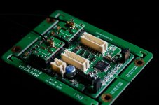
Ian,you can,show,confirms what it's the best way to connect the double XO board of Andrea to your both XO,please.
To make your clocks work with dual xo board
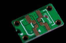
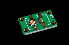
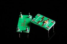
Hi andrea_mori,
I modified two xo adapters today and they look good.
I think you can use xo adapter PCBs to connect your clocks to dual xo clock board in the following way.
Please see pictures for details.
Merry Christmas!
Ian
Hi Ian,
since there are some fellow members who would like to use external XO with your dual XO board, and other who would like to use external dual XO with your FIFO buffer and I2S to PCM converter,
please, can you advise them how to do the job in this thread?
http://www.diyaudio.com/forums/digi...phase-noise-jitter-crystal-oscillator-25.html
Thanks
Andrea
Hi andrea_mori,
I modified two xo adapters today and they look good.
I think you can use xo adapter PCBs to connect your clocks to dual xo clock board in the following way.
Please see pictures for details.
Merry Christmas!
Ian
Attachments
Hi andrea_mori,
I modified two xo adapters today and they look good.
I think you can use xo adapter PCBs to connect your clocks to dual xo clock board in the following way.
Please see pictures for details.
Merry Christmas!
Ian
Hi Ian,
thanks for your time and your support, great as always.
Have a happy new year.
Andrea
- Home
- Source & Line
- Digital Line Level
- Asynchronous I2S FIFO project, an ultimate weapon to fight the jitter