Schematic attached. If you reuse the structure, you will need two of those, each connected to both inputs, but with opposite polarity. The ground level of the auxiliary op-amps can be changed, for example to match input offsets in the OPA1632. I propose increasing the resistor values to have higher input impedance and less loading on the main opamp.Yes, I'm open for other ideas. Unfortunately I don't know the DACmagic from the insides. Could you point me towards schematics or an analysis.
Well, if you don't have any input buffering, the OPA1632 will see the input common-mode. Especially if the source is distorted (some pro gear might expect the next stage to be very immune to common-mode) or the XLR cable picks something up, this might affect you. Also, if your input is single-ended, this might affect sound quality badly. There are enough eval boards and commercial products with bad implementations, so I advise you to go with your own common sense instead of looking at what others do.Well, maybe I'm just a little bit reluctant to use the fully differential amp as the first (input) and only (anti-aliasing filter) stage. But as I see from a lot of evaluation boards and commercial products, there seems to be no reason to be afraid of doing so. That's why I made a modification to the schematic (see attachment).
--
Greetz,
MatchASM
Attachments
Well, if you don't have any input buffering, the OPA1632 will see the input common-mode.
Of course, that's the job (and struggle) for any input stage. The main question is wether the OPA1632 is up to it - and I guess it is. Let me explain:
If I do have input buffering, the buffers are the ones that get to see the input common-mode. It's not obvious to me as to why shifting the problem to the prior stage would make solving it any easier. It's still common-mode, the buffers are still opamps, still having limited specs.
The OPA1632 is specified for a common mode input voltage range of -12.5V to +14V for a +/-15V supply voltage. That's half of what you get with a high impedance buffer, still it's way more than what most sources present. I could live with that, especially considering that even instrumentation amplifiers and differential receivers don't surpass this. As the input is protected (clamped) internally, I don't see any risk from common mode input, just possible distortion from overloading the diff stage. If in doubt, just clamp with additional zeners.
Especially if the source is distorted
If the source is distorted, then there's no hope to regain the original signal. For any type of input stage, thus I guess this is not what you meant. In case you refer to unwanted DC bias due to asymmetric distortion I don't see how the resulting common mode voltage could surpass the source's supply voltage. Within the +/-12V range the OPA1632 will damp this down by about 90dB (resulting in ~0.4mV output common-mode), above this range the clamps will just pass on the distortion.
(some pro gear might expect the next stage to be very immune to common-mode)
I don't intend to use pro gear that shows such behaviour, nor do I see the necessity to protect against any and all problems imaginable.

The only situation where this type of problem arises is with high source output impedance (like instrument effects gear or DI boxes), a property that isn't to be expected in quality line level interconnections.
Besides this, gear that delivers ill defined common mode behaviour can't be expected to deliver good noise immunity at the same time, thus sound would be degraded anyway.
It's usually the (truly) proven pro gear that is actually free of such symptoms, i.e. any transformer coupled output. Even low budget gear incorporates regular low-impedance drivers (like opamps) and balanced output circuitry (like in Behringer's DCX circuit itself, similar to Rod Elliot's Balanced Line Driver, fig. 2).
or the XLR cable picks something up
The balanced cable run picking up common mode voltage is to be expected! That's why balanced runs are preferred, as they (ideally would) make any noise pickup common mode instead of differential.
I still don't see the difficulties (with common mode input voltage) that an instrumentation amplifier would not have at or around unity gain...
Also, if your input is single-ended, this might affect sound quality badly.
True, but only because the circuit is DC coupled, as any DC component that is imposed on the input signal would now be amplified and passed through. The most widespread solution against this problem is capacitor coupling at the input, I'd rather prefer a high quality blocking capaciter after the input stage. My quality recommendation would be transformer coupling and proper cabling, although capacitor coupling is a lot easier and cheaper. See Jensen notes AN003 and AN004 as well as Rane Note 151, fig. 5 for further details.
I'd also assume that using the OPA1632 as a balanced input stage is similar to choosing any differential to single ended input receiver like INA134, a widely accepted choice in this type of application.
There are enough eval boards and commercial products with bad implementations, so I advise you to go with your own common sense instead of looking at what others do.
Understood.
But I still don't see the culprit with common mode distortion in this application. I'm aware of the reduced impedance level at the inputs, but it's still appropriate for the intended application.
Please also keep in mind that the DAC input is fully balanced with it's own CMMR specs, i.e. it has an internal high pass filter that elminiates any DC offset within it's own common-mode range.
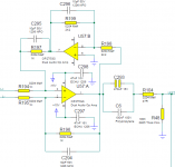
Schematic attached.
I perceive it as a differential to single ended converter with servo balanced biasing and capacitor output AC coupling.
If you reuse the structure, you will need two of those, each connected to both inputs, but with opposite polarity.
My idea was to reduce complexity, not increase it...
Now, applying two of them to the input of a fully balanced opamp would theoretically increase CMMR with the added benefit of offset control and AC coupling. Interresting idea, ideally the common-mode reduction ratios of the buffers and the balanced amp would add, as the balanced amp only sees the common-mode output of the buffers - which is the input common mode attenuated by their CMMR.
It's practical application looks difficult, though. The frequency compensation and transfer function doesn't look suitable to leveraging the OPA1632 in the next stage, also complicating calculation and making the whole thing more prone to component quality and tolerances (as imbalances in the two buffer circuits' transfer functions will greatly deteriorate CMMR of the following stage, probably beyond the point of making the gained CMMR futile).
Take a look at the attached schematic. It's Behringers original differential input buffer and AC coupling. That's basically your proposal minus the actively driven feedback loop (and plus rubbish components). Cloning this stage and reversing the input feeds towards the pair would theoretically yeld the same CMRR increase, yet it's never used. I can only explain this observation with difficulties that likely come with mirroring it's behaviour.
Lastly, that Vocm capability of the OPA1632 is a feature that renders control of absolute offset voltage unnececcary, as the output will be elevated to the (constant, input independent) ADC bias level anyway. Also, I don't see the need for input or output offset cancellation in this balanced, DC eliminating ADC drive application. Can you please elaborate? I might as well be wrong on this, it's been a weekend full of hard work at work.
Cheers,
Sebastian.
Attachments
I'm glad you finally got around to mentioning the VCOM pin, ; a fantastic feature that solves most of what you are talking about previous to that point as that is the whole reason its there. provided errors are common mode, which given a reasonably well realized diff cct is entirely possible; the result will be very acceptable. I love this chip along with others in its family, the SQ is as good as it is handy IMO. also if you use the package with the pad on the underside the current capability is quite high
Last edited:
I'm glad you finally got around to mentioning the VCOM pin
Only now did I mention it, but look how I prepared to use it from the beginning by extending the signal from the pin in the schematic.
It's the "VOCM" pin, btw.: output common-mode.
The fun property is that the Vocm input voltage replaces the output DC component of the (differential) input signal, independent of gain and frequency compensation. The block diagram (see attachment) shows that this is actually realized by something like a tapped servo loop...
provided errors are common mode, which given a reasonably well realized diff cct is entirely possible; the result will be very acceptable.
That's also my reason for choosing it. It sounds like you know it, then. How would you solve the input stage? What would be reasonably well realized according to you?
Attachments
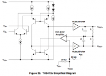
It's what it says it is, the simplified block diagram of the THS4031.
The similarities between the THS403x series (generic ADC driver) and the OPA1632 (specified for audio) are no secret, AFAIK. At least not since TI got into the DIY news when licensing parts of it from Nelson Pass.
It's not the holy grail of audio nirvana, but it gets the job done pretty fine I suppose...
PS: Andrew, I'm really interrested in your input regarding my buffer stage uncertainty.
Last edited:
I am starting to refer to balanced connections as balanced impedance connections.
Many Members do not realise that the advantages of balanced are thrown away if the send and receive impedances are not balanced.
The circuits showing +IN & -IN with different receive impedances are not balanced impedance.
Some believe that common mode impedance does not need to be matched, but I can't get my head around the physics of that stance.
correct I stuffed up the acronym ;D I admit I didnt start far back, I just read MatchASM's long post and then yours addressing his and was surprised at how long it took to be mentioned considering it makes much of the discussion irrelevant. i'm no expert at design, but I have a fair bit of experience with this chip and its brethren such as THS4151 (from memory, so many numbers in my little brain) in other peoples designs.
these chips are very similar to the pass susy designs, in fact Ti had to pay Nelson some dollars for using his patent so to speak (i'm not privy to the details) and its this servo that is at the heart of it, so you might have a look for some of these discrete designs for inspiration.
I would not presume to be able to tell you how to design your cct, i'm only just starting to play around with my own designs now and up till now have relied on the brains of others to create them, only exercising judgement on what I feel works best for my purpose and taste, mixing and matching, often modding. I dont know much about the design of this ADC, or ADCs in general and have only used these as dac output stages, despite them actually being designed for ADC. I would look at what AVCC/2 is for your ADC units, do they operate on a common mode level that is half the supply voltage and if so, sample that voltage and drive it into VOCM pin with a quality single instrumentation amp with very low input offset; then let the servo do its work on the output.
as far as the input filters that can be a bit tricky with differential designs due to the tolerance of even high quality caps (resistors arent a problem given enough money, so I would tend to try to do any filtering inside the OPA1632 feedback loop to keep any error to a minimum.
I do understand you correctly here in that you are looking to use this to drive the to drive the INPUT?
I am starting to refer to balanced connections as balanced impedance connections.
I am referring to balanced impedance as an equal impedance as seen from inverting and from non-inverting in- or output.
The circuits showing +IN & -IN with different receive impedances are not balanced impedance.
Yep!
BTW, do you see this in any of my schematics attached here?
Many Members do not realise that the advantages of balanced are thrown away if the send and receive impedances are not balanced.
Well, some differentiate.
For an interconnection to be fully balanced, the inverting and the non-inverting current paths need to be equal in transmitter output impedance, gain/damping, transmission line frequency response/transfer function and receiver input impedance.
They do not necessarily need to have equal transmitter impedance and receiver impedance, i.e. 50 Ohm output impedance and 50 Ohm receiver input termination, respectively. This would of course be advantageous to high frequency signal transmission (RF) like an AES/EBU digital audio connection, but it's absence does not ruin the gained common-mode reduction due to the symmetry.
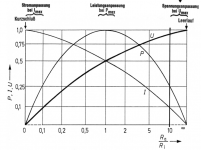
I have attached a diagram of input vs. output impedance. It's published by Eberhard Sengpiel on his website, I unfortunately couldn't find an English source for that kind of illustration (and I don't support all opinions of Sengpiel).
It shows voltage (U), current (I) and power (P) against impedance ratio of output impedance (Ra) divided by input impedance (Ri).
The extreme cases are short circuit ("Kurzschluß") at Ra/Ri = 0 and idle ("Leerlauf") at Ra/Ri -> inf.
Inbetween lies the range having maximum power transmission ("Leistungsanpassung").
As can be seen from the logarithmic ordinate, the relationship changes pretty quickly.
Consequentially, fitting a low output impedance transmitter to a high input impedance receiver almost universally makes any audio interconnection a case of "voltage fit" in the attached diagram. It's almost never a power fit and virtually never a short circuit.
Those are for transmission lines and power feeds.As of my understanding, going balanced and going for matched input and output impedances are two entirely independent design decisions, whereas the case Ra = Ri is entirely misplaced in the (analog) audio interconnection world due to established standards and proven best practice.
Cheers,
Sebastian.
Attachments
correct I stuffed up the acronym ;D
Yes, sorry, I've probably just been happy that I knew something.
have only used these as dac output stages, despite them actually being designed for ADC.
I'm also interested in using the balanced opamps in the output stage. It goes without saying that established DIY work will be my baseline. Members have used the OPA1632 in the output of the DCX2496, even in this thread.
I would look at what AVCC/2 is for your ADC units, do they operate on a common mode level that is half the supply voltage and if so, sample that voltage and drive it into VOCM pin with a quality single instrumentation amp with very low input offset; then let the servo do its work on the output.
The DAC in the DCX is the AK4393. It has a common mode output that would be suitable to driving the Vocm input, if only Behringer hadn't closed it off on the PCB. I assume it's not worthwhile to tap Vcom off the AK4393s on the DSP board and route a separate wire to the input board. I guess generating a well filtered AVCC/2 drive will probably be sufficient and less prone to noise.
as far as the input filters that can be a bit tricky with differential designs due to the tolerance of even high quality caps (resistors arent a problem given enough money, so I would tend to try to do any filtering inside the OPA1632 feedback loop to keep any error to a minimum.
It's being done with the THS/OPA we're discussing, although TI goes a bit over the top with their proposal in the PCM4222 reference design schematic. The most promising design I have seen for antialias filtering is with passive RC filters before and after the OPA1632. But a single cap in the feedback path won't hurt. Please note that I incorporate another passive pole after the OPA1632 and no audio filter (but a single pole rfi suppressor) preceding it.
I do understand you correctly here in that you are looking to use this to drive the to drive the INPUT?
Yes, this attempt is for the input stage. The Output stage will be attempted as soon as this very input stage is set.
haha I left the above post half finished while I had something to eat, I see you also mentioned the same pass vs Ti and the THS series ha
Ha, cool!
Let's rap.
No matter what the datasheet says, all opamps to some degree exhibit overshoot and measurable HF distortion rise due to the common-mode level at the input differential pair. Looking at your latest circuit diagram, I see that both inputs see resistors into a differential virtual ground. This is already quite good.
Could you please explain this to me?
I have to disagree. If only one pin carries the signal, half of the input signal becomes common-mode.
I would tend to disagree here also.
Yes, but I urge you to remove the output AC coupling and DC couple to the summing resistors at the OPA1632 input. Also, you probably know better opamps than the OP275.
Let me then first thank you for taking the time to reply so sensibly after so much hard work. However, the VOCM will not have an influence on the different DC-levels at the input arising from input pair offset. IIRC, the OPA1632 input offset specs are not spectacular. And this offset will translate to a DC operating point with differential imbalance. This will mean asymmetric loading of the source and more influence of the VOCM loop on the output signal. With a buffer you would not get rid of the asymmetric loading of the source, but you would have manual control over the way the common-mode is rejected. I'm pretty sure that if you do it by dummy opamp it will be better than with the OPA1632. I suggest you try both ways and see for yourself what the difference is to your ears (I always use a friend with better hearing than myself to tell me such things; also this automatically makes it a blind test...).
So, although the datasheet says the CM loop is very good (and in theory this should eliminate the need for any input buffering), IMHO you should expect it to have high-frequency intermodulation effects and keep this in mind when designing a circuit.
In conclusion, Behringer original (vastly <<) your proposed circuit (potentially even <) your circuit with added DC servo input buffer.
--
Greetz,
MatchASM
Of course, that's the job (and struggle) for any input stage. The main question is wether the OPA1632 is up to it - and I guess it is. Let me explain:Well, if you don't have any input buffering, the OPA1632 will see the input common-mode.
If I do have input buffering, the buffers are the ones that get to see the input common-mode. It's not obvious to me as to why shifting the problem to the prior stage would make solving it any easier. It's still common-mode, the buffers are still opamps, still having limited specs.
The OPA1632 is specified for a common mode input voltage range of -12.5V to +14V for a +/-15V supply voltage. That's half of what you get with a high impedance buffer, still it's way more than what most sources present. I could live with that, especially considering that even instrumentation amplifiers and differential receivers don't surpass this. As the input is protected (clamped) internally, I don't see any risk from common mode input, just possible distortion from overloading the diff stage. If in doubt, just clamp with additional zeners.
No matter what the datasheet says, all opamps to some degree exhibit overshoot and measurable HF distortion rise due to the common-mode level at the input differential pair. Looking at your latest circuit diagram, I see that both inputs see resistors into a differential virtual ground. This is already quite good.
That's not true; even-order harmonic distortion will be cancelled by a balanced-to-unbalanced stage.If the source is distorted, then there's no hope to regain the original signal. For any type of input stage, thus I guess this is not what you meant. In case you refer to unwanted DC bias due to asymmetric distortion I don't see how the resulting common mode voltage could surpass the source's supply voltage. Within the +/-12V range the OPA1632 will damp this down by about 90dB (resulting in ~0.4mV output common-mode), above this range the clamps will just pass on the distortion.
Noted.I don't intend to use pro gear that shows such behaviour, nor do I see the necessity to protect against any and all problems imaginable.(some pro gear might expect the next stage to be very immune to common-mode)
Besides this, gear that delivers ill defined common mode behaviour can't be expected to deliver good noise immunity at the same time, thus sound would be degraded anyway.
Could you please explain this to me?
The balanced cable run picking up common mode voltage is to be expected! That's why balanced runs are preferred, as they (ideally would) make any noise pickup common mode instead of differential.or the XLR cable picks something up
I still don't see the difficulties (with common mode input voltage) that an instrumentation amplifier would not have at or around unity gain...
True, but only because the circuit is DC coupled, as any DC component that is imposed on the input signal would now be amplified and passed through. The most widespread solution against this problem is capacitor coupling at the input, I'd rather prefer a high quality blocking capaciter after the input stage.Also, if your input is single-ended, this might affect sound quality badly.
I have to disagree. If only one pin carries the signal, half of the input signal becomes common-mode.
I'd also assume that using the OPA1632 as a balanced input stage is similar to choosing any differential to single ended input receiver like INA134, a widely accepted choice in this type of application.
I would tend to disagree here also.
I perceive it as a differential to single ended converter with servo balanced biasing and capacitor output AC coupling.Schematic attached.
Yes, but I urge you to remove the output AC coupling and DC couple to the summing resistors at the OPA1632 input. Also, you probably know better opamps than the OP275.
It still comes down to two dual opamps as in your earlier schematic, but now only two amps are directly in the signal path. Of course I do not argue with your conclusion that five opamps are more than one.My idea was to reduce complexity, not increase it...If you reuse the structure, you will need two of those, each connected to both inputs, but with opposite polarity.
I do not understand what you mean here.It's practical application looks difficult, though. The frequency compensation and transfer function doesn't look suitable to leveraging the OPA1632 in the next stage, also complicating calculation and making the whole thing more prone to component quality and tolerances (as imbalances in the two buffer circuits' transfer functions will greatly deteriorate CMMR of the following stage, probably beyond the point of making the gained CMMR futile).
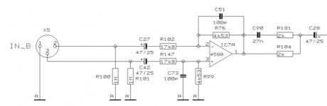
No, this schematic is fundamentally different and probably much worse than your proposal without any input buffer. The input resistor at the + terminal of the op-amp goes to ground and not a dummy -1 node. This means that there will be voltage swing on the + terminal, or common-mode, which will cause CM-induced distortion of the op-amp. And by the looks of it, quite a lot actually.Take a look at the attached schematic. It's Behringers original differential input buffer and AC coupling. That's basically your proposal minus the actively driven feedback loop (and plus rubbish components). Cloning this stage and reversing the input feeds towards the pair would theoretically yeld the same CMRR increase, yet it's never used. I can only explain this observation with difficulties that likely come with mirroring it's behaviour.
Lastly, that Vocm capability of the OPA1632 is a feature that renders control of absolute offset voltage unnececcary, as the output will be elevated to the (constant, input independent) ADC bias level anyway. Also, I don't see the need for input or output offset cancellation in this balanced, DC eliminating ADC drive application. Can you please elaborate? I might as well be wrong on this, it's been a weekend full of hard work at work.
Let me then first thank you for taking the time to reply so sensibly after so much hard work. However, the VOCM will not have an influence on the different DC-levels at the input arising from input pair offset. IIRC, the OPA1632 input offset specs are not spectacular. And this offset will translate to a DC operating point with differential imbalance. This will mean asymmetric loading of the source and more influence of the VOCM loop on the output signal. With a buffer you would not get rid of the asymmetric loading of the source, but you would have manual control over the way the common-mode is rejected. I'm pretty sure that if you do it by dummy opamp it will be better than with the OPA1632. I suggest you try both ways and see for yourself what the difference is to your ears (I always use a friend with better hearing than myself to tell me such things; also this automatically makes it a blind test...).
So, although the datasheet says the CM loop is very good (and in theory this should eliminate the need for any input buffering), IMHO you should expect it to have high-frequency intermodulation effects and keep this in mind when designing a circuit.
In conclusion, Behringer original (vastly <<) your proposed circuit (potentially even <) your circuit with added DC servo input buffer.
--
Greetz,
MatchASM
Hello,
This may be answered somewhere in the thousands of posts to this thread. Please point me in the correct direction.
If recall correctly the preferred location for the volume control is outside the digital box, this is to maximize the S/N ratio and not control loudness by the number bits used.
I am using amplifiers with balanced inputs and volume control at each of six amplifiers. I want to set and leave these input pots.
Is there an aftermarket bolt-on balanced analog control that will install between the output of the DCX 2496 and the power amplifiers?
DT
All just for fun!
Correct, either use digital in or analogue at a preset level to maximise bit usage.If recall correctly the preferred location for the volume control is outside the digital box, this is to maximize the S/N ratio and not control loudness by the number bits used.
Jan Didden did one for the DCX which replaces the output board and has volume control and remote.I am using amplifiers with balanced inputs and volume control at each of six amplifiers. I want to set and leave these input pots.
Is there an aftermarket bolt-on balanced analog control that will install between the output of the DCX 2496 and the power amplifiers?
http://www.linearaudio.nl/6chan-1.htm.
It's too expensive for me as I need 3 of them, so designed my own and I'm not aware of any other external commercial VC that does balanced I/O.
No matter what the datasheet says
Well yes, of course I don't just look at the datasheet.
I'm aware that any kind of common-mode input might cause distortion due to effects like making the diff pair leave their optimal bias point, some CCS getting modulated, thus inducing IMD into the next stage, and many evil things more.
It's just that I'd like to leave the effort in an acceptable range, not going into excess complexity. But I certainly see your point, maybe I should just try and compare the three configs (unbuffered, buffered, servo-buffered) in my application. If only time wasn't flying...
Looking at your latest circuit diagram, I see that both inputs see resistors into a differential virtual ground. This is already quite good.
Are you referring to post #2900? That was my latest schematic, although it's the one without the buffers.
That's not true; even-order harmonic distortion will be cancelled by a balanced-to-unbalanced stage.
If the common-mode range of a preceding stage is surpassed and it distorts, going unbalanced in a subsequent stage will cancel out the even order components? I don't think so, but even if it did, there's no point, as the distortion will likely be nonlinear.
Could you please explain this to me?
At this point I was referring to gear with 'ill defined' common mode behaviour and claimed that this usually comes with bad noise immunity. By that I was referring to noise caused by high impedance drive and/or bad cabling or signal routing. If you look at the diagram in my last post #2909 these would be cases left of Ra/Ri = 10, i.e. where SNR would be degraded while common-mode distortion would be unaffected, thus rising in proportion. Another type is ruined balancing, i.e. due to unequal impedance levels, bad contacts, non-parallel routing, etc.
I have to disagree. If only one pin carries the signal, half of the input signal becomes common-mode.
I'm assuming balanced cabling when interconnecting unbalanced sources to my balanced input. Some ways to do this can be seen in the application notes I linked to above (Jensen, Rane).
Only one wire carries the signal, but both wires carry the common-mode distortion. Thus, while only one input pin receives the input signal (i.e. half the input level, thus half the SNR), still both pins receive the common-mode voltage collected from output to input. As for this common-mode voltage, the full CMRR applies (I misspelled it 'CMMR' previously, sorry).
So, of course half of the input signal becomes common mode. Thus the halving of the output level. But what I didn't agree with was the remark that single ended drive would affect sound quality badly. It can be worse due to the lost balance in the impedances, but that's also true for the differential buffers.
I would tend to disagree here also.
As you might have guessed, I don't have insight knowledge into balanced receiver circuits.
But I have worked with the usual suspects from Analog and Burr Brown. Those are not instrumentation amplifiers, but basically opamps in differential input topology with with highly precise component matching.
What can SSM2143 or INA134 do that OPA1632 cannot be made to do, component precision aside (i.e. assume 0.1% resistors)?
I do not understand what you mean here.
The disadvantages due to the higher complexity might outweight the benefits. At least for someone without an RF PCB fab...
I'm pretty sure that if you do it by dummy opamp it will be better than with the OPA1632. I suggest you try both ways and see for yourself what the difference is to your ears (I always use a friend with better hearing than myself to tell me such things; also this automatically makes it a blind test...).
Yeah, I'm beginning to realize that I probably won't get around extensive prototyping. I see dead bug style projects coming.
So, although the datasheet says the CM loop is very good (and in theory this should eliminate the need for any input buffering), IMHO you should expect it to have high-frequency intermodulation effects and keep this in mind when designing a circuit.
Thanks, an essential point of insight gained!
In conclusion, Behringer original (vastly <<) your proposed circuit (potentially even <) your circuit with added DC servo input buffer.
Ahhh, that's a judgement I can work with.
As of my understanding, both a differential pair (as built into the OPA1632) and an instrumentation amplifier (as would be had with the input buffer stage in front of the OPA1632) are capable of rejecting common-mode input voltage.
Now, the in-amp does a much better job at presenting a very high input impedance to a source. At the same time, smart dealings with the differential inputs of the buffer opamps could further increase common mode rejection over what OPA1632 offers on it's own.
The tradeoff that I see is this: the differential buffers with the inverter in it's feedback loop has a much higher component count, first and foremost a second opamp (in the feedback loop), but also a far higher count of passives (compensation, etc.) with their own tolerances. To be fair, we're comparing this to simple voltage followers in the classic in-amp, having a passives count of zero.
The more I think of it the less I like the idea of being the first to try joining this approach to a balanced opamp directly driving an ADC. Twofold.
As desperate as it might make me look, I feel like my original question is still unanswered: Is the diff pair and the distortion behaviour of the OPA1632 enough for the intended application (directly driving the AK5393 in the DCX) or do I have to configure them as instrumentation amplifiers to really leverage on using this topology at the input?
I will try both alternatives. But I'm prepared for the possibility of not recognizing a difference. In such cases I prefer to base my decisions on science, best practices and experience (of others). So?
Thanks!
I've used mine bone stock until recently, when I exchanged the opamps in some of the output channels. I tried Philips NE5532 and TI OPA2134 against the stock Cool Audio V4580.
The eyeopener for me: that funny NJM4580 rippoff was absolutely competetive.
It's the power supply and the circuit topology (together with bad signal routing and some other pitfalls) that are to blame for the high noise level and the dull sound at low input levels.
That's when I started to look into alternatives and found this thread...
you may have misunderstood my meaning when I said send and receive to have balanced impedances. I did not mean equal impedances.................
For an interconnection to be fully balanced, the inverting and the non-inverting current paths need to be equal in transmitter output impedance, gain/damping, transmission line frequency response/transfer function and receiver input impedance.
They do not necessarily need to have equal transmitter impedance and receiver impedance, i.e. 50 Ohm output impedance and 50 Ohm receiver input termination, respectively.
The transmit hot and cold source impedances must be balanced.
eg 50r+-0.1% & 10uF+-1%
The receive end could be 1M5+-0.5%//10k+-0.1%//220pF+-1%.
Tighter tolerances can be adopted if you have the resources.
- Home
- Source & Line
- Digital Line Level
- Behringer DCX2496 digital X-over