Originally by analogspiceman:
I suspect this design approach is most often used in place of understanding rather than to enhance it.
I'll admit to that to a certain extent, I got real sick of trying to figure out all the little spice quircks and bugs, just to get a basic sim going rather than those of the circuitry itself. That's just a general spice comment, aimed at none in particular, but I did start with workbench, so welcome to that nightmare. The frustration was immense.
Having no scope or anything component level sims also served me well to get an actual amp working, which the idealized model would have never done. It took alot of research, trial and simulation in order to take an educated guess at what was really going on with it, reproduce it with spice, or sometimes the problem was already there and I just wasn't looking, and then trying to fix it. That, I think brought me to a new level of understanding.
Just to say, it has its place too, and can enhance understanding! I guess it depends on the user?
But you're right, and I regard your post as digital gold, it's what the books and websites don't really explain well.
Thanks,
Chris
Originally posted by Chris (classd4sure)
I'll admit to that to a certain extent, I got real sick of trying to figure out all the little spice quirks and bugs, just to get a basic sim going rather than those of the circuitry itself. That's just a general spice comment, aimed at none in particular, but I did start with workbench, so welcome to that nightmare. The frustration was immense.
Having no scope or anything component level sims also served me well to get an actual amp working, which the idealized model would have never done. It took a lot of research, trial and simulation in order to take an educated guess at what was really going on with it, reproduce it with spice, or sometimes the problem was already there and I just wasn't looking, and then trying to fix it. That, I think brought me to a new level of understanding.
Never used it, but the "buzz" I've heard is that Workbench is worse than useless for serious work (supposed to be very friendly to those looking for an introduction to electronics and not familiar with SPICE syntax, though).
Spice, especially LTspice (which, because of its many enhancements, has never failed to run any circuit I've fed it) coupled with modern computing power, can just about replace the development lab, if one has some basic knowledge of electronics and is willing to wear a detective's hat now and then.
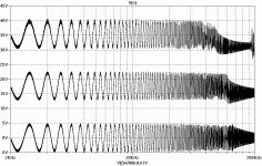
Attached is the output plot of the swept sine analysis posted earlier in this thread. Note how the dc level modulates the frequency response.
Regards -- analogspiceman
Attachments
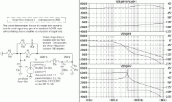
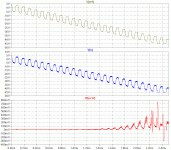
Here's an ac analysis for the component values in the feedback network of a UcD style design. As mentioned previously, this analysis can be very helpful for ensuring that the lead network in the feedback path provides enough phase lead margin around the resonant point of the LC output filter operating into an open circuit. Interestingly, most of the lead occurs past the sudden phase shift of resonance.
Regards -- analogspiceman
The attached image show an example of the above applied to an LTspice analysis of a UcD style amplifier.
Top Trace: the phase lead network response
Middle Trace: loop gain with nominal load (6 ohms)
Bottom Trace: open circuit loop gain
Regards -- analogspiceman
The attached image show an example of the above applied to an LTspice analysis of a UcD style amplifier.
Top Trace: the phase lead network response
Middle Trace: loop gain with nominal load (6 ohms)
Bottom Trace: open circuit loop gain
Attachments
Originally posted by analogspiceman
Have you ever examined the consistency of the small signal, high frequency square wave response (say a couple of volts peak at 10kHz) of your UcD design when summed with a large signal, low frequency triangle wave (say nearly rail to rail at 50 hertz or so)? This approximates the small treble riding on big bass of real music, but with a signal much more palatable to the "eye analyzer"

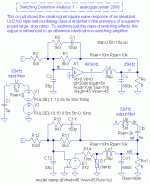
Okay, here is a simulation that does just that. It shows the small signal (10kHz) square wave response of an idealized UcD180 style self-oscillating class-d amplifier in the presence of a superimposed large (rail-to-rail), slow triangle wave. To give the amplifier a break and show only its audio band response, signals have been band limited to 32kHz (both the input waveform and the output switching distortion products are low pass filtered with a 2-pole, zero overshoot LCR section).
To make things really interesting, I have attempted to examine just the class-d switching effects with everything else subtracted out. An otherwise identical non-switching amplifier has been constructed and the outputs of both are differenced against each other and examined with switching ripple blocked out. Both amplifiers have the same gain and saturation characteristics, and both have nearly identical frequency shaping networks (the linear amp has no delay a very slight high frequency lead network to provide stability and keep it from switching). If I've set up the simulation correctly, the only signals left in the difference plots are the switching-caused in-band audio artifacts.
Should be interesting, yes?
Regards -- analogspiceman
First the simulation schematic...
Attachments
Originally posted by analogspiceman
[...] the only signals left in the difference plots are the switching-caused in-band audio artifacts.
First the simulation schematic...
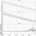
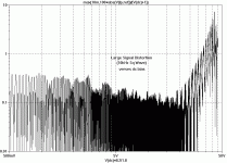
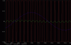
The top trace is the output of the non-switching amplifier (note that it saturates to the rail very much like the UcD output below it).
The middle trace is the UcD amplifier. It looks pretty clean except near the rails where the switching frequency becomes irregular.
The bottom trace is the audio artifact taken from the difference between the two amplifier outputs. For signals not too near the rails, there is very little distortion, but things do seem to break up a little bit near the edges, eh?
Regards -- analogspiceman
Now, the simulation output...
Attachments
Analogspiceman,
Excellent posts, it looks like I'll be spending some time with LTspice again today.
Thanks,
Sander Sassen
http://www.hardwareanalysis.com
Excellent posts, it looks like I'll be spending some time with LTspice again today.
Thanks,
Sander Sassen
http://www.hardwareanalysis.com
analogspiceman said:
The top trace is the output of the non-switching amplifier (note that it saturates to the rail very much like the UcD output below it).
The middle trace is the UcD amplifier. It looks pretty clean except near the rails where the switching frequency becomes irregular.
The bottom trace is the audio artifact taken from the difference between the two amplifier outputs. For signals not too near the rails, there is very little distortion, but things do seem to break up a little bit near the edges, eh?
Regards -- analogspiceman
Now, the simulation output...
Hi,
I love when you get bored.
Seems like your results on this one confirm mine. From what I gathered with not much work (easily be wrong) it seemed the increased ripple amplitude was to blame. I was thinking of experimenting with limiters in the feedback network.
Regards,
Chris
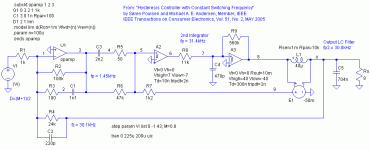
analogspiceman[/i] [B] If you mean this paper said:
If I'm not mistaken you are the primary author of the papers I referenced in the beginning of this thread. If so, I would very much appreciate it if you would email me the values used in the unreadable simulation schematics included in your papers that I referenced. You must have noticed that Bruno more or less blew off the claim made in the paper with regard to the superiority of a linearized hysteresis self oscillating class d amplifier as compared to the UcD style class d circuit. I would like to attempt to verify this claim using LTspice (hence the need for the values).
Never mind about emailing the values - Jaka Racman had access to a copy with better detail than the one I got from the IEEE, and he was kind enough to update me with the previously unreadable information.
") Thanks Jaka
Thanks JakaI still had to guess at several pieces to the puzzle, though. The inductor sense winding was not specified, the comparator and output stage voltage saturation voltages were missing as were their delay times. Oh, and the load.
The following values yield a fair match to the waveforms of your paper: an 8 ohm load, a 20 to 1 current transformer turns ratio (inverting), +/- 7 and 40 volts for the saturation levels, and 10 and 300ns for the comparator and output stage delays, respectively. (Without a realistic output stage delay the circuit doesn't seem to work at all.)
How'd I do, guess-wise?
(Please feel free to jump right in and correct me.)Regards -- analogspiceman
Here's the simulation schematic ...
Attachments
 I had no idea the circuit you were after was on that paper. The values in my copy are very readable as well!
Originally posted by analogspiceman
The bottom trace is the audio artifact taken from the difference between the two amplifier outputs. For signals not too near the rails, there is very little distortion, but things do seem to break up a little bit near the edges, eh?
Regards -- analogspiceman
Now, the simulation output...
I inadvertently forgot to reduce the effective loop gain of the non switching amplifier reference standard in the above comparison.
The UcD design actually looks significantly better than indicated above. When I get the time for it I will repost the correct results plus some more interesting data.
Regards and apologies to Bruno & Co. -- analogspiceman

How does the double-loop topology above simulate in terms of distortion ?
I am curious since I did simulations on an almost similar topology about two years ago.
The differences were that it was carrier-based and that it didn't sense the voltage accross the inductor.
I still have the material to build it but didn't find time to actually do it so far.
Regards
Charles
I am curious since I did simulations on an almost similar topology about two years ago.
The differences were that it was carrier-based and that it didn't sense the voltage accross the inductor.
I still have the material to build it but didn't find time to actually do it so far.
Regards
Charles
Originally posted by phase_accurate
How does the double-loop topology above simulate in terms of distortion ?
No idea ... yet. My first goal is to match the results of the original paper.
Only then can I play with the circuit to figure out the fundamental, key characteristics to its function, after which I can design a simplified version that more directly expresses the essence of that function. This will serve both a proof of understanding and allow me to compare its idealized version to that of the UcD style design.
If the soren posting here is the original paper's author, I really hope he joins in the fun.

Regards -- analogspiceman
Here's a zipped version of the LTspice .asc schematic file:
Attachments
Originally posted by analogspiceman
I inadvertently forgot to reduce the effective loop gain of the non switching amplifier reference standard in the above comparison.
The UcD design actually looks significantly better than indicated above. When I get the time for it I will repost the correct results plus some more interesting data.
Okay, gain has been reduced from 257 to 168 and the rest of the circuit is now exactly the same as the switching version (200ns delay back in and output zero lead network out).
Except near the rails, there is virtually no difference between the fully linear, non-switching amplifier and its UcD class-d brother.
Regards -- analogspiceman
Attachments
How about a load invariant frequency response? I find that to be one of the winning features of the UcD concept. Does the AIM concept provide this too?
Cheers,
Sander Sassen
http://www.hardwareanalysis.com
Cheers,
Sander Sassen
http://www.hardwareanalysis.com
Analog,
Just a couple of simulations setup questions
Are you running Method=Gear Solver=alternate?
I have to admit to being a novice when it comes to optimizing LTspice so I thought I’d ask an expert.
I normally simulate ClassD’s in LTspice with the following settings, any comment?
Max time step=1nsec
Method=Gear,
Solver = Alternate
Gmin=1e-12
Abstol=1e-14
Reltol=0.001
Chgtol=1e-14
Trtol=1
Voltol=1e-008
Sstol=0.001
I’ve also found that I need to crank down on Chgtol in circuits which rely on charge conservation.
Is there a better one setting “simulation=accurate” mode for LTspice?
BTW : great work posting all these ccts and putting it in a simulatable form (LTspice) where all interested amateurs have a chance to "understand" the problems and hopefully build on the knowledge base.
Classdunce
Originally posted by analogspiceman
Okay, gain has been reduced from 257 to 168 and the rest of the circuit is now exactly the same as the switching version (200ns delay back in and output zero lead network out).
Except near the rails, there is virtually no difference between the fully linear, non-switching amplifier and its UcD class-d brother.
Just to show the value of the presentation of data, I have reformatted the above to resemble a THD vs. Power curve. "Distortion" is taken as the absolute value of the residual difference signal divided by the dc bias level (plus one volt because of the 1Vp squarewave) and dc bias is displayed against a logarithmic x-axis (to scale like power).
I wonder how this compares to the real UcD 180's small signal distortion curve at 10kHz?
Regards -- analogspiceman
Distortion plot attached ...
Attachments
So I finally read the discussed paper (thanks S. !).
I think that comparing the circuit in the paper in question with the UcD is comparing apples to oranges. The paper shows an interesting approach to achieve constant frequency operation for hysteresis modulators. T
he UcD is a phase-shift oscillator that differs in behaviour. One main property is the intrinsically good frequency-stability compared to hysteresis modulators.
There are no clues regarding the performance of the prototype - apart form the switching frequency behaviour - in the paper. I think a suitable prototype for real audio amplification would have to be built in order to know how it behaves acoustically.
But it is definitley more complicated than the UcD which will not be easy to beat regarding performance and simplicity.
I have been in e-mail contact with another member recently. He is doing simulations and building test circuits using phase-shift self-oscillating topologies. This made me undig a simulation circuit that I once tried after reading B&O's "COM patent".
I haven't seen this circuit anywhere else so far - not even in the patent - but it might be covered by the claims in said patent(which are the most powerful part of a patent anyway). It is derived from the classic phase-shift oscillator.
If anyone is intersted I can post the details (maybe in a seperate thread).
Regards
Charles
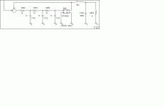
Below one could see the most basic implementation of the idea. It is a classic phase-shift oscillator with an inverting loop and a high- or low- passfilter as phase shifter. For our purpose a lowpass topology is advisible !
The gain-stage (Etable) has a gain of 100 and it saturates at + and - 1 Volt. The inversion is made with the subtracting stage - which is also used for the superposition of our audio signal.
Regards
Charles
The gain-stage (Etable) has a gain of 100 and it saturates at + and - 1 Volt. The inversion is made with the subtracting stage - which is also used for the superposition of our audio signal.
Regards
Charles
Attachments
- Status
- This old topic is closed. If you want to reopen this topic, contact a moderator using the "Report Post" button.
- Home
- Amplifiers
- Class D
- Is the UcD modulation scheme less than optimum?