Hi !
I've nearly sucessfully built my first ClassD, fully discrete using standard devices.
It plays like hell, but, i have some problems left..
First problem, without the 1nF in the VAS deadtime seems to be too short,
heating up the P-Channel...
The second problem, driver for opening the mosfets heats up, so i have to turn off after ~5 minutes.
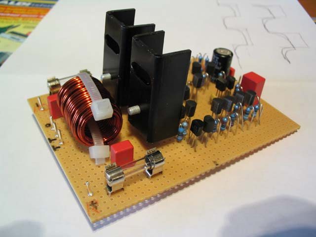
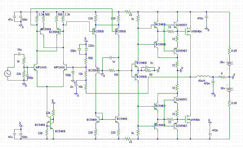
The schematic i've constructed:

The 0.05 ohms represent the fuses...
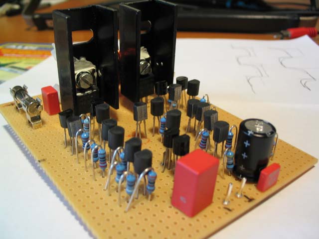
And the prototype: (not the latest)
Any ideas, suggestions ?
MikeB
I've nearly sucessfully built my first ClassD, fully discrete using standard devices.
It plays like hell, but, i have some problems left..
First problem, without the 1nF in the VAS deadtime seems to be too short,
heating up the P-Channel...
The second problem, driver for opening the mosfets heats up, so i have to turn off after ~5 minutes.
The schematic i've constructed:
The 0.05 ohms represent the fuses...
And the prototype: (not the latest)
Any ideas, suggestions ?
MikeB
Go ahead, discrete class D is great!...good luck!
Even with those little problems sounding good!...this is a promiss that will be very good when those details turned fixed.
regards,
Carlos
Even with those little problems sounding good!...this is a promiss that will be very good when those details turned fixed.
regards,
Carlos
Hi MikeB,
Have you tried increasing your final driver 33R emitter resistors? Maybe try just increasing the N-channel ones to something like 47 or 56R.
Have you tried increasing your final driver 33R emitter resistors? Maybe try just increasing the N-channel ones to something like 47 or 56R.
Hi subwo1 !
No, have not tried yet, but you're right, the n-channel is faster !
The 1st version used 10ohms, then i increased to 33ohms, but did
not show any change... 🙁 I will try !
What i do not understand, only the P-channel heats up, the N-channel
keeps cold, should crossconduction not heat up both ?
Mike
No, have not tried yet, but you're right, the n-channel is faster !
The 1st version used 10ohms, then i increased to 33ohms, but did
not show any change... 🙁 I will try !
What i do not understand, only the P-channel heats up, the N-channel
keeps cold, should crossconduction not heat up both ?
Mike
Beautiful prototype!
About that P-channel heating, have you matched your mosfets? I suppose you did, but maybe they have drifted...
About that P-channel heating, have you matched your mosfets? I suppose you did, but maybe they have drifted...
Hi Giaime !
I did not really match the mosfets, i only matched them for identical
Vgs-threshold... I can't avoid having different Rds-ON, also the
p-channel has higher recoverytimes, but i have no idea how to
measure that !
Mike
I did not really match the mosfets, i only matched them for identical
Vgs-threshold... I can't avoid having different Rds-ON, also the
p-channel has higher recoverytimes, but i have no idea how to
measure that !
Mike
Originally posted by MikeB [some snippage]
I've nearly successfully built my first ClassD, fully discrete using standard devices. It plays like hell, but, i have some problems left.. First problem, without the 1nF in the VAS deadtime seems to be too short, heating up the P-Channel... The second problem, driver for opening the mosfets heats up, so i have to turn off after ~5 minutes.
And the prototype: (not the latest)
Any ideas, suggestions?
Since your output inductor is a coreless solenoid, it may be injecting enough stray flux back into your amp to cause problems. As a test, space it back on the end of a twisted pair of wires, 20 or 30 cm away from the rest of the circuitry.
I don't suggest it, but as a test to demonstrate how much trouble this inadvertent coupling can cause, you could then bend it back down very close over your circuit board, moving it and twisting it around until your circuit starts misbehaving (and probably breaks).
Regards -- analogspiceman
PS: What did you mean by "VAS"?
MikeB said:What i do not understand, only the P-channel heats up, the N-channel
keeps cold, should crossconduction not heat up both ?
One thing that could heat the P-channel more is its greater rds-on. But like you were thinking, it would also seem to me that both should heat up, still. It may have something to do with the P-ch's body diode recovery being forced by the N-ch. Maybe something will occur to me later.
Hi analogspiceman !
Hmm, i hoped the heatsinks would give some "shielding"...
A bit dumb, as the heatsinks are made of alloy...
Would it be enough for testing to put some steelplate between
coil and rest of amp ?
With "VAS" i meant the 2nd diffamp with currentmirror, loaned from
another ClassAB-design. With the 150ohm the voltageswing is
reduced to +/- 1.2volt, also giving low zout. The 1nF slows down this
signal, and with the 0.6v vbe-threshold of the following bjts i "cut"
this signal at it's half, giving ~100ns deadtime.
Mike
I don't know if this is your problem, but 36 volts of gate drive is probably not good for those output transistors... At least not in the long run. But i guess puncturing the gate oxide would be more terminal than just heating up. Like Short and Kaboom!
Okay, here's a few things I missed by looking at your post, the schematic and the prototype:
- Coil needs to be shielded as mentioned by a few others already
- Did you match the transistors in the frontend?
- Try thermally coupling the driver transistors to the mosfets.
- Esp. in the switching stage the transistor gain should be identical on both the N and P side, so at least match those else the output will skew or slant.
Best regards,
Sander Sassen
http://www.hardwareanalysis.com
IRF9540 and IRF640 are a better complementary match for just about any parameter you care to name except maximum Vds 😉
Also, you appear to be driving your gates with up to full rail voltage, 36V? Vgsmax is usually +-20V.
Even if the MOSFETs could take more than 20V, you need to limit the positive swing, you are only unnecessarily charging the gate and transfer capacitance which are not small, which will make it much more difficult for the MOSFET to turn off. 9V Vgs should be more than enough for double the maximum current through these devices even at 150C junction temperature.
Slightly better turn off characteristics could be had if your driver stages MOSFET turn-offs were suppied a few V higher rails, this will give the driver transistors a bit more headroom to turn the MOSFET off completely. Your predriver stage can source a huge base current for the turn-on drivers (in theory only the 50 ohm resistor is the limit!), but only a small current for the turn-off drivers as this is furnished via the 1k resistor. To make things worse, as Vgs decreases during turn off, the base current decreases as well, given you have a 2xVbe voltage drop there, and given that you should insure gates get 2V or lower to be turned off (to insure they turn off when outputs are hot - not often in class D but you want to be sure!), you only get 1ma base current (and that's being optimistic) - keep in ming you may be trying to pull ampere pulses out of the MOSFET gate. Lowering gate drive by appropriately dividing the voltage via extra resistors in the predriver stage, you may end up being able to lower the 1k resistor and solve two problems at the same time. Alternatively, you can use current sources instead of the 1k resistors but then you absolutely need the extra driver rails due to the minimum voltage needed for the current source to work.
Hi !
Thanks for the response !
About the Vgs, it's typically about 8-10volts (measured with scope),
but you are right, it should have zeners to protect against some overshoots...
The current through the 1k in front of the drivers is ~9ma.
The transistors in frontend are matched, but i have to try to make some
idle measurings to be really sure.
Especially the "schmitt-trigger" would not like unmatched bjts...
Ilimz, i'm also not completely happy with the 2xvbe for switching off,
but i had to use doubledriver because of the 1k delivering the basecurrent
for switching off. Maybe i could use some CFP-style ?
I think the driverstage could be heavily improved, also the choice
of devices might be bad... But bd139/140 showed heavy ringing in sims.
I will replace the coil, but will need a few days to order some
ferriterings or ready coils. I did this aircoil because i had enough
wire, but no ferrite, and wanted to start off with building.
Also this one will not saturate easily...
At least the TV-picture did not show signs of heavy EMI when
i turned on the amp... 😀 (I already had ClassAB-amps doing this...)
I already replaced the irf9540n, for the case i had a bad device,
but nothing changed...
Mike
MikeB said:About the Vgs, it's typically about 8-10volts (measured with scope), but you are right, it should have zeners to protect against some overshoots...
How? It cannot be that low unless your schematic is not accurate - a quick calc by hand reveals tha the input of the predrivers can swing about +-2.2V, since your predriver gain is ~~200 (OK, optimistic but still...), you have to get more than 10V at the drivers.
You could simply limit the swing by increasing the emitter resistor of the predriver (and decreasing the 1k in front of the drivers).
You didn't give the approximate frequency so I can't tell how much the 1n cap changes things but unless it's limiting gain, I still can't see Vgs only 10V? If it is, and the schematic is accurate, it must be by pure luck...
MikeB said:The current through the 1k in front of the drivers is ~9ma.
Maybe while Vgs is 10V, it is, but for lower Vgs, the voltage on these resistors has to lower, therefore also current. Since you have a double driver and need less than 2.2V or thereabouts to reliably turn off the MOSFET, 2.2V - 2xVbe ~~ 1V at the base of the drivers, at that point current through 1k is 1mA. Any current into B of the drivers will just make matters worse and further decrease the ability of the driver to turn the MOSFETs off.
MikeB said:Ilimz, i'm also not completely happy with the 2xvbe for switching off, but i had to use doubledriver because of the 1k delivering the basecurrent for switching off. Maybe i could use some CFP-style?
I think the driverstage could be heavily improved, also the choice
of devices might be bad... But bd139/140 showed heavy ringing in sims.
I think the devices are OK - if more current is needed you could always parallel two of the second drivers. The ones you are using are much faster than BD139/140, and have higher gain, which is what you want here. Maybe you could also try BC337/327? But that 1k just doesn't seem right - have you checked the current waveform in it with the simulator, and also the current waveform for the turn off transistors in the driver?
BTW something just occured to me - which manufacturer made your IRF9540N?
Hi MikeB,
I have more thoughts about why the P-ch is heating more than the N-ch. The timing of the gate drive in relation to the stored energy of the choke determines whether or not it is able to charge or discharge the capacitance at the MOSFET drains before a MOSFET turns on. The more the MOSFET itself must change the capacitance voltage during its the lossy turn-on time, the greater its power dissipation.
During certain output power, pulse width, and timing situations, there can be plenty of stored energy to change the voltage on the capacitance at the drains from one rail to the opposite one, while other times there can be more than enough to go in one direction while almost none to go the other way. However, the prerequisite is that each MOSFET must be off and not dissipating the choke energy during its lossy transition time from on to off. Right there could be the problem--the P-ch may be turning off too slowly.
Since your feedback is taken before the filter try breaking the connection to the output choke to see if both MOSFETs heat. Also, as I see it, the reason your MOSFET gates may not be getting overdriven is the loading effect of the 150R from the VAS output to ground. Best Regards.
Hi ilimz !
Okay, here is the "exact" calc for the Vgs:
The gain of the predriver/levelshifter is ~14, given a virtual additional Re
of 20ohms you get 1000/(50+20) = 14. The currents delivered by "vas" are ~8ma,
this gives voltageswing of 1.2volts because of the 150ohms to ground.
1.2volts minus vbe is ~0.65v, *14 -> 9.1v. Or, 0.65v to 70 ohms = 9.3ma.
I made this construction to create plenty of deadtime, the 1nF "rounds" the
edges of the squarewave, if i now subtract 0.6v from this "degraded" signal,
i get a "gap" of ~100ns. The 1nf in paralell to the 150 ohm is not big enough
to limit the gain, it only smoothes the signal a bit.
These 1.2volts are verified with scope.
The oscillationfreq is ~308khz (measured). Sims predicted 320khz.
So i am quite sure that there is no problem with too high gatevoltage, sometimes
sims are surprisingly accurate. (At least with bias calculations, not with timings)
But, it all seems to be the problem with too slow switching off, maybe the signal
is simply to much degenerated in the vas ? I think i can partially improve
the signal by adding a 1nf in paralell to the 50 ohms Re. At least in sims this
technique works perfect, it improves the signal again to 50ns rise/fall, bigger
caps create overshooting. Also i will reconsider the driverstage.
Theoretically both mosfets are IRF, but you never know what you really get...
Both mosfets have the same labeling, using the IRF-brand, the IR with the diode
between. But they costed only 60cents...
Subwo1, as i understand you, the turn off is simply too slow, this means i have
crossconduction through both mosfets, but with the irf540n beeing "more powerful",
it forces down the voltage to -supply while crossconduction is happening, giving
very high dissipation to the p-channel, while the n-channel is only dissipating
what is created by it's Rds-on ?
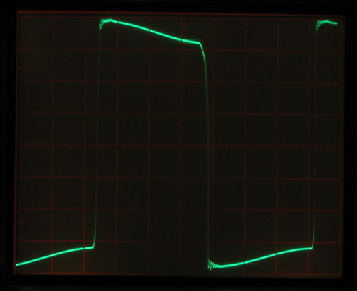
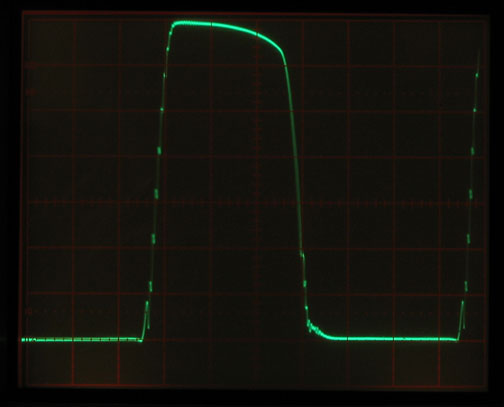
I attached a shot from sims, green is switchoffcurrent, red is switchon, blue is
current through 1k. Maybe i really should improve switchon ?
Improving switchoncurrent would also reduce heating of the driver, as more of the
disspation would be moved to the 33ohms...
Mike
Okay, here is the "exact" calc for the Vgs:
The gain of the predriver/levelshifter is ~14, given a virtual additional Re
of 20ohms you get 1000/(50+20) = 14. The currents delivered by "vas" are ~8ma,
this gives voltageswing of 1.2volts because of the 150ohms to ground.
1.2volts minus vbe is ~0.65v, *14 -> 9.1v. Or, 0.65v to 70 ohms = 9.3ma.
I made this construction to create plenty of deadtime, the 1nF "rounds" the
edges of the squarewave, if i now subtract 0.6v from this "degraded" signal,
i get a "gap" of ~100ns. The 1nf in paralell to the 150 ohm is not big enough
to limit the gain, it only smoothes the signal a bit.
These 1.2volts are verified with scope.
The oscillationfreq is ~308khz (measured). Sims predicted 320khz.
So i am quite sure that there is no problem with too high gatevoltage, sometimes
sims are surprisingly accurate. (At least with bias calculations, not with timings)
But, it all seems to be the problem with too slow switching off, maybe the signal
is simply to much degenerated in the vas ? I think i can partially improve
the signal by adding a 1nf in paralell to the 50 ohms Re. At least in sims this
technique works perfect, it improves the signal again to 50ns rise/fall, bigger
caps create overshooting. Also i will reconsider the driverstage.
Theoretically both mosfets are IRF, but you never know what you really get...
Both mosfets have the same labeling, using the IRF-brand, the IR with the diode
between. But they costed only 60cents...
Subwo1, as i understand you, the turn off is simply too slow, this means i have
crossconduction through both mosfets, but with the irf540n beeing "more powerful",
it forces down the voltage to -supply while crossconduction is happening, giving
very high dissipation to the p-channel, while the n-channel is only dissipating
what is created by it's Rds-on ?
I attached a shot from sims, green is switchoffcurrent, red is switchon, blue is
current through 1k. Maybe i really should improve switchon ?
Improving switchoncurrent would also reduce heating of the driver, as more of the
disspation would be moved to the 33ohms...
Mike
Hi MikeB, I think it is a combination of factors. At that switching frequency, the turn-off needs to be fast since that is when the inductor releases its energy. If a MOSFET is in the extra resistive state between on and off, the choke flyback energy will be dissipated in the MOSFET. During turn--on, the choke has high impedance, so most of any dissipation will come from either shoot-through or changing the voltage on the capacitance at the drains. Turning on a MOSFET faster makes shoot-through worse and may make losses from driving capacitance worse as well.
Update
Hi !
I had some sucess with adding a 3nf to the Re of predriver/levelshifter.
Driver is much colder, so is the p-channel. It seems that the signal
was too degraded for proper switching...
Updated schematic:
Scopeshot of output before coil: y: 10v/div
You can see that the energy of the outputchoke is stored in the 470nF.
Scopeshot of Vgs p-channel: y: 2v/div (upside down)
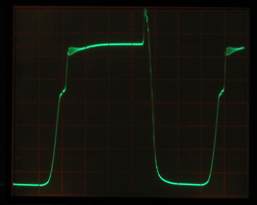
Scopeshot of Vgs n-channel: y: 2v/div
All Scopeshots have x: 0.5us/div
I will try to improve the driverstage, as the pchannel-vgs shows some
"stucking" when vgs drops below 4volts... Also there is some ringing in the vgs.
Mike
Hi !
I had some sucess with adding a 3nf to the Re of predriver/levelshifter.
Driver is much colder, so is the p-channel. It seems that the signal
was too degraded for proper switching...
Updated schematic:
Scopeshot of output before coil: y: 10v/div
You can see that the energy of the outputchoke is stored in the 470nF.
Scopeshot of Vgs p-channel: y: 2v/div (upside down)
Scopeshot of Vgs n-channel: y: 2v/div
All Scopeshots have x: 0.5us/div
I will try to improve the driverstage, as the pchannel-vgs shows some
"stucking" when vgs drops below 4volts... Also there is some ringing in the vgs.
Mike

- Status
- Not open for further replies.
- Home
- Amplifiers
- Class D
- My fully discrete ClassD