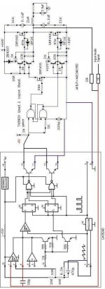
Here is the schematic layout of my recently completed Class-D amp with using discrete Gate drivers using MJE350/340 transistors.
The Frontend includes
LM3524D Pulse Width Modulator
Nand Gate with deadtime insertion
Gate drivers
Output half bridge stage
Filter
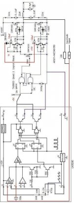
The Frontend includes
LM3524D Pulse Width Modulator
Nand Gate with deadtime insertion
Gate drivers
Output half bridge stage
Filter
Attachments
Reply
The frequency response i get is 10Hz To 18Khz
Secondly
The HIP4081 or HIP4080 are meant to operate only at 80Volts maximum supply voltage.
What If some wants a AMP with supply Rails of an order of +-95VDC
Thirdly I am in INDIA and discreteness is my destiny thats why i have choosen the discrete gate drive for simplicity and cost effective ness
Blow-up for certain.
Replace the IN4007 with an ultra-fast diode like BYV26C or similar. But even more important, the floating rail that this diode pumps will get jolted to 56 volts when the lower fet turns on!!! WAY too much for the upper fet gate. Perhaps run the top of the diode to a ~15 volt or so ground referenced supply, and use 100uF across the floating driver rail in addition to what is there now. (can't see it while writing this).
Other than that, Good Man!
Edit -> Oh yeah, I see. The upper fet gate at most is only going to get as high as the +56v rail. The fet will never fully turn on, unlike the lower one. Spells even-harmonic distortion.
I understand your concerns about using "standard" discrete components. But I have some doubts about the performance of your high-side driver:
You don't limit the supply voltage of this driver which could in turn be dangerous for the driven Mosfet.
I don't know how fast the upper Mosfet can be turned on with this "VAS" using a mosfet and a pullup resistor.
Why do you use modulators that work with a sawtooth instead of a triangle ? Didi you ever attempt a switching amp that takes feedback from the output filter ?
Regards
Charles
Ok. Now I have the schematic open in a second window...
Run the top of the 1N4007 instead to the +12v supply on the lower driver. (you could probably raise it to 15 volts) Also, the 10k pullup resistor for the IRF630, shift it from the anode to the cathode of the 1N4007. This will make sure that the upper fet gate can be pulled above +56 volts. You might need to fiddle the value of this 10k, probably lower it quite a bit, 1k at a guess. If it is too high the IRF630 drain rise time will be too slow.
That's it.
If it is too high the IRF630 drain rise time will be too slow.
That's what I wanted to say. Maybe a "speedup" circuit could be built with a bootstrap cap from the output of the high-side complementary driver-pair.
Regards
Charles
 Gotta go. In the meantime, tell us all how those suggestions go.
amp man
Dear Amp Man i made a d class amplifier for my final project on the university 3 years ago, in half bridje but i tried every conbination posible and for that range of output power i recomend to work in full bridge and using IRF540N, Is the best in Ciss, faster than the others an most eficient.
Dear Amp Man i made a d class amplifier for my final project on the university 3 years ago, in half bridje but i tried every conbination posible and for that range of output power i recomend to work in full bridge and using IRF540N, Is the best in Ciss, faster than the others an most eficient.

I took another glimpse at the circuit and the data sheet of the modulator IC and I first thought it couldn't work (because the output signal is toggled from one output to the other one in order to drive half-bridge PSUs coorectly). Then I saw that your outputs are used as wired OR.
So I believe that it should work in pronciple. But I am not convinced that a high quality amp can be built with such a modulator IC.
Assuming that you have actually built it: What are your distortion figures (at which carrier frequency ?) and how does it sound ?
Regards
Charles
So I believe that it should work in pronciple. But I am not convinced that a high quality amp can be built with such a modulator IC.
Assuming that you have actually built it: What are your distortion figures (at which carrier frequency ?) and how does it sound ?
Regards
Charles
- Status
- This old topic is closed. If you want to reopen this topic, contact a moderator using the "Report Post" button.
- Home
- Amplifiers
- Class D
- Class-D Amp with Discrete Gate Drivers