As you all saw, my class d modules do not intefer with a FM tuner, but they do seem to interfer with each other.
each module on its own has little noise but as soon as i bring the second module into operation the noise level increases quite a bit, and it also seem to go up and down, sometimes with a little bit of crackle and hum in it, and sometimes barely even audible from a meter away.
This is why i put on the ferrite thingies, but they had little to no effect, separating the gate drive to a isolated supply for each module reduced the hiss alittle.
It turns out these modules are a perfect full signal AM station!! PCB layout FAIL!
Well Thats a shame you were getting there.
Anyway the last design you made didn't have a proper two layer PCB board and you didn't have copper guard tracks around critical switching nodes to reduce EMI.
Before you abandon ship take pictures of Vgs, Vds ect (something i never seen you done 😕) .. build a small loop ring loop antenna and hoover it over the EMI areas to perform RFI analysis.
You need to experiment with things to see what improves things or makes them worse.
You could try a ground sheet of aluminium between the pcb's to see if it is a radiated or conducted emissions problem.
I use to try extra decoupling.
Also the separate pcbs need star grounding from each other if using the same supply.
I have just finished a high power valve amplifier and I found that good earthing was vital to low noise.
nigelwright
"Star Grounding" is a class AB mentality, EVA has spoken about this many many years ago... its no good for fast high speed class D designs. in fact ive never seen high speed PCB designs even use that term "star grounding" in applications.. look at track guards, modelling inductance this is real high speed design terminology and practices.
Class D or SMPS tend to use ground planes.
Star grounding applies to multiple amps running off the same supply.
Star grounding applies to multiple amps running off the same supply.
Latest design was indeed a dual layer thing with a as unbroken as possible ground plane on the bottom with decoupling caps as close to the ic power pins as possible. And guard traces would be useless as this UcD design is supposed to have some kinda level of the switching frequency present everywhere, audio input included.
I know about guard traces, its a trick to prevent a node carrying a noisy signal from coupling to a nearby trace which could be the input of a opamp amplifying a mic signal or something of that nature inside a stereo with a class d amp on the same board to prevent the class d from coupling noise into the mic line, however i've never seen guard traces used in any class d amplifier i ever seen so far.
Due to my limited scope bandwidth i call any Vds/Vgs measurement useless as ringing is more or less always way above 20MHz, as i dont even see the ringing i should see from the inductance in the ground lead. And if my problems were ringing based, i'd expect a FM tuner to stop working near the amp which it dident, it only had a slight effect on a weak station that wasent listenable to begin with.
If someone wants to donate a 100MHz or more bandwidth scope i'd gladly take the offer. This is another reason to quit class d for the time beeing, until i have the proper hardware, i once had a 100MHz tek but it developed some fault which the error code hinted toward the trigger circuitry, i couldent be bothered trying to find the fault so i dumped it at a former friends place.
I deleted all pics of the bare boards as i dident want anyone to copy this inferior layout, but now it looks like i may have to take new pics of both sided of a board for troubleshooting purposes.
😛 i don't think so.Class D or SMPS tend to use ground planes.
Star grounding applies to multiple amps running off the same supply.
Start grounding refers to the common reference ground point, all grounds points are referenced from that point in a "star" like shape hence the term star.
its used in AB amplifiers to reduce ground loop hums ect..
http://www.diyaudio.com/forums/power-supplies/115698-understanding-star-grounding.html
Latest design was indeed a dual layer thing with a as unbroken as possible ground plane on the bottom with decoupling caps as close to the ic power pins as possible. And guard traces would be useless as this UcD design is supposed to have some kinda level of the switching frequency present everywhere, audio input included.
I know about guard traces, its a trick to prevent a node carrying a noisy signal from coupling to a nearby trace which could be the input of a opamp amplifying a mic signal or something of that nature inside a stereo with a class d amp on the same board to prevent the class d from coupling noise into the mic line, however i've never seen guard traces used in any class d amplifier i ever seen so far.
Due to my limited scope bandwidth i call any Vds/Vgs measurement useless as ringing is more or less always way above 20MHz, as i dont even see the ringing i should see from the inductance in the ground lead. And if my problems were ringing based, i'd expect a FM tuner to stop working near the amp which it dident, it only had a slight effect on a weak station that wasent listenable to begin with.
If someone wants to donate a 100MHz or more bandwidth scope i'd gladly take the offer. This is another reason to quit class d for the time beeing, until i have the proper hardware, i once had a 100MHz tek but it developed some fault which the error code hinted toward the trigger circuitry, i couldent be bothered trying to find the fault so i dumped it at a former friends place.
I deleted all pics of the bare boards as i dident want anyone to copy this inferior layout, but now it looks like i may have to take new pics of both sided of a board for troubleshooting purposes.
If you go into high speed PCB designs here is a good book im reading at the moment its on my desk and i think its very good.
High Speed Digital Design: A Handbook of Black Magic
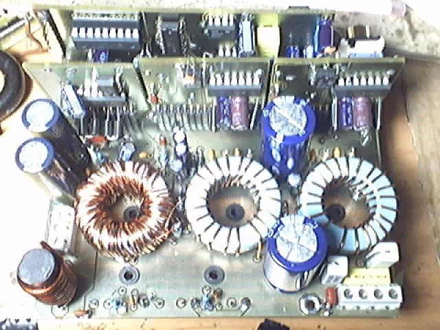
so heres some pics for troubleshooting:
http://i.imgur.com/lXphc9P.jpg
http://i.imgur.com/Lfpz8G5.jpg
http://i.imgur.com/lXphc9P.jpg
http://i.imgur.com/Lfpz8G5.jpg
so heres some pics for troubleshooting:
http://i.imgur.com/lXphc9P.jpg
http://i.imgur.com/Lfpz8G5.jpg
Good quality components poor arrangement why is the LC section so near the signal processing area?? it almost sitting on top of the gate driver.😕
I thought the output filter should be as close to the fets as possible with as short trace from the Vds junction as possible, and i figured the gate drive was relatively unsensitive to the emi from the output inductor.
This layout was pretty much inspired from how the hypex UcD180ST is laid out except i put the comparator on the main board instead of on a daughter board.
However prioblems with the inductor beeing too close to stuff would be a noisy amp, not a AM transmitter. But if you think the coil is too close, i can replace it with one of those used on the sure audio irs2092 based class d that look like a ferrite block, i assume those are fully shielded and have little to no field leakage.
I thought the output filter should be as close to the fets as possible with as short trace from the Vds junction as possible, and i figured the gate drive was relatively unsensitive to the emi from the output inductor.
This layout was pretty much inspired from how the hypex UcD180ST is laid out except i put the comparator on the main board instead of on a daughter board.
However prioblems with the inductor beeing too close to stuff would be a noisy amp, not a AM transmitter. But if you think the coil is too close, i can replace it with one of those used on the sure audio irs2092 based class d that look like a ferrite block, i assume those are fully shielded and have little to no field leakage.
I would be careful with referencing the design on Hypex. they using a 4 layer design i think and the modulator is enclosed in expoy a few cm away from the modulator with a RM core. RM physically seem more enclosed as well they not using toroidal cores.
Look at this this is a good layout
See how far the LC filter is from the modulator..
An externally hosted image should be here but it was not working when we last tested it.
Last edited:
The pictures are helpful but can you show raw layout and schematic graphic files too? Some traces are hard to see, like where the logic ground pin 13 goes, and a few others.
The raw layout files were deleted hours ago and garbage bin has already been emptied.
From what i can tell from pictures of a UcD180 module, its dual layer board, not a four layer board.
So it turns out i laid out my board as wrong as possible, ie i did nothing right.
From what i can tell from pictures of a UcD180 module, its dual layer board, not a four layer board.
So it turns out i laid out my board as wrong as possible, ie i did nothing right.
I have made a new try at a layout but i guess this one is as terrible as the previous one, if not worse.
Better or worse ? You decide: http://i.imgur.com/jJolGOl.png
Better or worse ? You decide: http://i.imgur.com/jJolGOl.png
I added caps everywhere, but im pretty sure this is still incorrectly laid out is just as bad as the previous layout, if not worse.
Better or worse ? You decide: http://i.imgur.com/26AsL5q.png
Better or worse ? You decide: http://i.imgur.com/26AsL5q.png
I found a highly interesting video about EMC:EMC Testing - YouTube
So heres my conclusion of the source of my problems:
So heres my conclusion of the source of my problems:
Attachments

That will not exactly have helped (To say the least, you see lots of this form of broken in class AB designs where one can mostly get away with it).
Now also consider the loop from the earthy side of the filter capacitor to the HF decoupling caps by the fets.., you probably loose little in moving the bulk electrolyics a little further away if it lets you fit some more SMT 1206 or 1210 100n caps right at the power inputs to the mosfets.
Splits in the ground plane are generally a really bad thing, as they can dramatically increase loop area, doing a polygon pour on the track side of the board and via stitching it to the ground plane so as to provide a short path across any splits in the plane will help (Not as much as not splitting the plane in the first place, but it will help).
A small ferrite (Wurth do some nice chip inductors for this) or sommon mode choke in the speaker connections together with a few hundered pF of shunt cap will help reduce the higher harmonics where that film cap is doing little due to lead inductance.
SMT is generally better behaved then leaded when it comes to parasitics.
Just my immediate thoughts.
Regards, Dan.
Atleast it has alot less breaks in the ground plane than the version i have problems with.
As i am working on this i am looking at a pic of a UcD180ST module, it does only have a single pair of ceramics right at the fets just like my version, it does not have the lil ferrite thing on the speaker output you suggest as shown in this version of the layout.
Ideally i'd like to get the vreg cirs for the comparator moved to the same side of the board as the big power traces as the way it is now i'd get currents from the zeners flowing through the same ground path as audio, potentially causing extra noise, also like i have it now i still get that same huge loop area as i had on the problem version due to where the vreg cirs are.
Attachments

Looks like you're whittling it down there Tekko. Seek to minimize all the local loops and try to get everything spun around so that the common gets distributed in a radial fashion even though you're using a ground plane, with only the short local loops hanging out very far. Your first update posted in #33 looked like the same thing to me. With no reference it was hard to tell anyway. Try to get it down to the point where you can't do Anything better. Little stuff like even turning the zeners around (though you've already moved them) so that the ground point is next to the caps instead of spread around. That wont make much difference but it's something that is clearly possible...an example. The big deal is the signal and power reference spread, and leaving things in the middle that either catch or inject noise along the way. I haven't seen a schematic so it's difficult to make more specific suggestions.


- Status
- Not open for further replies.
- Home
- Amplifiers
- Class D
- Increased noise with multiple modules