Because of pumping , you'll need a very expensive powersupply to run it. BTL is prefered.
If china would make this we would get professionally looking PCB cheaply. Power Supply is not a problem and is the user responsibility.
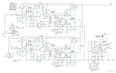
Are there any flaws in these 2k to 4.5k watt boards?
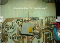
Need schematic explaination
Hello,
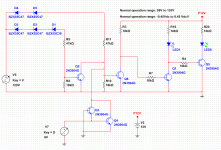
I need to know the way in which the LM311 is used in the schematic shown in post 1 and 4 of this thread.
1. The comparator output is tied to +3V rail and the output is taken from the ground pin connected to -3V through a 470E resistor. What is this arrangement doing?
2. If I replace IR2110 with a half bridge driver that has only one PWM input, can I use the LM311 with pin-1 tied to GND and pin-7 driving the half bridge driver, thus eliminating the circuit based around the four transistors?
Hello,
It seems like the protection section needs a lot of work. I think the OTP, OVP and UVP needs a re-look.
regards,
bimbla.
hi bimbla pls post a reviewed ot,oc,ovp schema.
hi bimbla pls post a reviewed ot,oc,ovp schema.
I don't use OTP, but here is the scheme for UVP, OVP and DCP. Based on the amplifier control circuit topology this can be universally adapted to any amplifier.
Attachments
For what do you need them ?here is the scheme for UVP, OVP

It must be the prerogative of the SMPS...........
hi all i have used this schematic with success at +/-85vlts at 2ohms irfb4227 with success i wanted to use high voltage +/-120vlts with irfb4229 with a 4 ohm load is it possible????
hi all busy perfecting smps and ucd semi discreet .that is lm 311 and ir2110 in ucd amp. all is well the amp is o.k and cool even at 2 ohms
but ocp protections are the ones holding me back .i have made lorylaci ucd version with protection ,it works well but trips very soon / early. i think when the amp is 60% loud . i wanted it to reach about 92% at 2ohm per channel because i wanted to use full bridge +/-70vlts fets used are a pair of irfb4227 per channel
any help some one??. the schematic ic below and my layouts are below.Attachments
-
 gtG ucd 1100 rev 1.0 with protect semi smd.jpg225 KB · Views: 1,366
 -
 gtG ucd 1100 rev 1.0 with protect semi smd bottom.jpg207.2 KB · Views: 1,292
 -
gtG ucd 1100 rev 1.0 with protect semi smd schematic.pdf45.8 KB · Views: 324
-
gtG ucd 1100 rev 1.0 with protect semi smd components 2.pdf234.8 KB · Views: 291
-
gtG ucd 1100 rev 1.0 with protect semi smd pcb bottom.pdf37.9 KB · Views: 214
-
gtG ucd 1100 rev 1.0 with protect semi smd pcb top.pdf29.4 KB · Views: 225
-
 600W Class D amplifier ucd_ir_hid_jav.jpg185 KB · Views: 1,311
I was looking at your NeoD2K v0.6b schematic. I was stuck at the current limit circuit in the +ve and -ve supply rails and was wondering if the -ve current limit will be triggered at the much higher current than the +ve value because of D22.
Also, would it be better if the volume control is followed by a buffer rather than an inverting gain stage?
regards,
bimbla.
Hi
Dont really bother how much precise current during short circuit. There is plenty current stored in the supply supply cap. As this is momentary only. And your mosfet usually has very high transient current capability.
It means for mine I can set trip at quite high overcurrent and OCP still working and safe. I use 2x0.1ohm sensor resistor. Need to generate 0.7V to trigger ocp transistor high or low side.
Many people even best engineer too focus on how much current to trip if my supply is at some amps. No.... not to be perfectly like that.
Sorry to all of you that I am too busy with work
My schematic is tested. But I cannot share pcb.
I use ltspice.
The schematic is scalable output depend on voltage supply. It has been tested upto 130Vdc live with mosfet IRFP4242. And change cap supply to be 160V and 400V for cap plus to minus. Also R shunt replaced with 20K 5W
For all kind this schematic, like iraudamp1 or detex version, if you find dc offset or at worse very bad pumping which may cause supply unbalance, the problem is resistor at emmiter of 2N5401 need to be adjusted. This kind of topology has weakness at the level shifter that shall be perfecfly balanced.
- Home
- Amplifiers
- Class D
- UCD 25 watts to 1200 watts using 2 mosfets