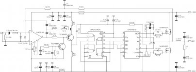
DA2 CD4070 is comparator stage, in original (iraudioamp) was used another logic.Which stage is intended to work as a comparator?
DA2 CD4070 is comparator stage, in original (iraudioamp) was used another logic.
 its not a comparator stage
Comparator can be represented as a usual hi-speed opamp, even with not very high amplification coefficient. And we have here the stage T1 plus one XOR element, providing relatively high amplification coefficient. So it will work similar to comparator without any problems. Sure, input offset voltage of T1+XOR is 'not ideal', but this will be compensated by input integrator easily.
I think this schematic will work...
Also, be careful, the switching freq can be too high, because delay producing by DA2 is not so big. Maybe I would inlcude one more free XOR element of DA2 into the path to produce more delay, even more helping DA2 to act as a comparator
I will only say, that the UcD topology is more preferable, if it is not a commercial development. UcD will give more stable switching frequency and better performance results... Simply replace DA1 with a comparator IC (T1+XOR will be not enough here
), replace your feedback with a UcD style feedback and it will be a UcD amp!
Last edited:
Comparator can be represented as a usual hi-speed opamp, even with not very high amplification coefficient. And we have here the stage T1 plus one XOR element, providing relatively high amplification coefficient. So it will work similar to comparator without any problems. Sure, input offset voltage of T1+XOR is 'not ideal', but this will be compensated by input integrator easily.
I think this schematic will work...
Also, be careful, the switching freq can be too high, because delay producing by DA2 is not so big. Maybe I would inlcude one more free XOR element of DA2 into the path to produce more delay, even more helping DA2 to act as a comparator
I will only say, that the UcD topology is more preferable, if it is not a commercial development. UcD will give more stable switching frequency and better performance results... Simply replace DA1 with a comparator IC (T1+XOR will be not enough here
Do you even know what comparator does?
Comparator can be represented as a usual hi-speed opamp, even with not very high amplification coefficient. And we have here the stage T1 plus one XOR element, providing relatively high amplification coefficient. So it will work similar to comparator without any problems. Sure, input offset voltage of T1+XOR is 'not ideal', but this will be compensated by input integrator easily.
I think this schematic will work...
Also, be careful, the switching freq can be too high, because delay producing by DA2 is not so big. Maybe I would inlcude one more free XOR element of DA2 into the path to produce more delay, even more helping DA2 to act as a comparator
yes, and you?

CD4070 XOR is used as PHASE SPLITTER OF PUSLES [for driving the gate driver chip]not a comparator, opamp is already acting as integrator and comparator simuntaneously

I have only blown my output stage once with an high supply voltage around 190V (and 13200uF of low ESR caps). I was doing power testing and I was in another room with two closed doors and two concrete walls inbetween, yet I could hear the bang in detail.
The result was a lot of vapourized PCB (thick polygons, not just tracks), exploded TO-220 cases, vapourized TO-220 leads, and some small SMD parts disappeared.
And this happened with a quite mature design, not just the first prototype.
In other words, be careful
btw: Your design lacks many important things.
btw2: An high-speed op amp can't do the work as a hi speed comparator, and vice-versa. A comparator is a one bit analog to digital converter. An op-amp is intended to produce an analog output. Comparators exhibit very high gain and slew rates at the expense of the inability to make them work in a NFB loop. 5mV of overdrive are enough to change the state of the outputs completely within a few dozen nanoseconds.
Last edited:
Comparators exhibit very high gain and slew rates at the expense of the inability to make them work in a NFB loop. 5mV of overdrive are enough to change the state of the outputs completely within a few dozen nanoseconds.
Put 5mv overdrive to the hi-speed opamp inputs, and it will change it's state very fast too
The only differences between op-amps and comparators I see is the special cares to avoid a deep saturation of BJT devices inside of a comparator and avoidance of any phase corrections (making them unable to work with NFB).
And famous LT1016 does not have a very high gain, actually it has even less gain than any other precise op-amp...
CD4070 XOR is used as PHASE SPLITTER OF PUSLES [for driving the gate driver chip]not a comparator, opamp is already acting as integrator and comparator simuntaneously
I know very good, what the CD4070 is intended in this schematic for
But if you say, that the CMOS element does not have any gain, then please explain, how it is possible to build crystal oscillators using it...
Last edited:
Can any of your high speed op-amps produce full 50Mhz square wave output with 5mV of overdrive on the input?
High speed comparators can. They can't be made stable with NFB because they keep the high gain up to very high frequencies, unlike op-amps. Gain at DC may not be as high as in op-amps, but there are no poles on it until very high freqencies.
High speed comparators can. They can't be made stable with NFB because they keep the high gain up to very high frequencies, unlike op-amps. Gain at DC may not be as high as in op-amps, but there are no poles on it until very high freqencies.
I never said that cmos is not having any gain, all i told you was that the application of cd4070 in that schematic was for phase splitter rather than a comparator.I know very good, what the CD4070 is intended in this schematic for
Put 5mv overdrive to the hi-speed opamp inputs, and it will change it's state very fast too
The only differences between op-amps and comparators I see is the special cares to avoid a deep saturation of BJT devices inside of a comparator and avoidance of any phase corrections (making them unable to work with NFB).
And famous LT1016 does not have a very high gain, actually it has even less gain than any other precise op-amp...
Can your hi speed opamp could switch in less than 10nS????
Comparators are mostly known by RESPONSE TIME which is of importance and in opamps the response time doensnt matters that much.
Given that the TL081 op amp used is not "fast" at all, the first XOR gate will act as a comparator, something that a CMOS gate is not intended to do, since the analog input level, always close to 2.5V, may result in high dissipation in the gate due to prolonged cross conduction.
I use CMOS gates as 1/2 Vcc comparators sometimes, but only when the input voltage is going to be far from the commutation threshold most of the time. The circuit can't rely on the threshold being exactly at the center either.
I use CMOS gates as 1/2 Vcc comparators sometimes, but only when the input voltage is going to be far from the commutation threshold most of the time. The circuit can't rely on the threshold being exactly at the center either.
Last edited:
Can your hi speed opamp could switch in less than 10nS????
would this hi speed op-amp have no any phase correction networks inside and would this op-amp have some shottky diodes between base and collector of BJT devices to avoid their saturation, then it would be able to do this... But in general, they are the same...
And please notice, that the CMOS gates are not having any saturation effect Also, CMOS elements of CD4000 series are not having low Rdson, so it is not so dangerous to feed their inputs with Vcc/2 at all. But the HC74 series may indeed overheat and die in such case.
Greetings!
I have returned
It is glad that the circuit will work. There was one more question: what power(W) can be received with a +/-100V supply if to include such two amplifiers the bridge?
I have chosen tl081 for experiment because of its low cost if the circuit will earn that I am going to put something better ad817, ad8001 for example
It will be better agree that ucd but here is how it to make here while precisely I do not know, can share as better to transfer the given circuit in ucd It is possible sent on my personal email: vogor@yandex.ru
Thanks for answerrs 2 all.
I have returned
It is glad that the circuit will work. There was one more question: what power(W) can be received with a +/-100V supply if to include such two amplifiers the bridge?
I have chosen tl081 for experiment because of its low cost if the circuit will earn that I am going to put something better ad817, ad8001 for example
UcD will give more stable switching frequency and better performance results... Simply replace DA1 with a comparator IC (T1+XOR will be not enough here
It will be better agree that ucd but here is how it to make here while precisely I do not know, can share as better to transfer the given circuit in ucd
It is possible sent on my personal email: vogor@yandex.ruThanks for answerrs 2 all.
- Status
- This old topic is closed. If you want to reopen this topic, contact a moderator using the "Report Post" button.
- Home
- Amplifiers
- Class D
- Self-oscillating class D amplifier