No wonder
No wonder they are so jumpy on my boards! Still, you have 8 channels bridged and only 4 adjusters. If the pot isn't maxed out then as good as it gets is as good as it gets.Hello Scott,
You have the the 2x100 board and 2 trimmers, the 4x100 board has 4 trimmers, still one per channel. There are no 100k resistors on the 2x100 board, they are coarse but they do work.
5mV
Ok. So, I just tried all 3 of my 2X100 boards and was able to get them all set to within +-5mv.
Ok. So, I just tried all 3 of my 2X100 boards and was able to get them all set to within +-5mv.
Audio1st we have a DC-offset of 0mv on all channels!!! thank you so much for your advice on those resistors! once they were shorted the trim pot became a lot more sensitive and i was then able to dial out the offset.
I have yet to actually remove the resistors as i have currently painted them with Electrically conductive paint which has worked great, i am not so sure how this will effect the long term if i was just to leave it this way, rather than removing and bridging with solder.
Once again thank you very much!!! i can now continue with fitting the board into an enclosure.
Merry Christmas,
Craig
Hi,
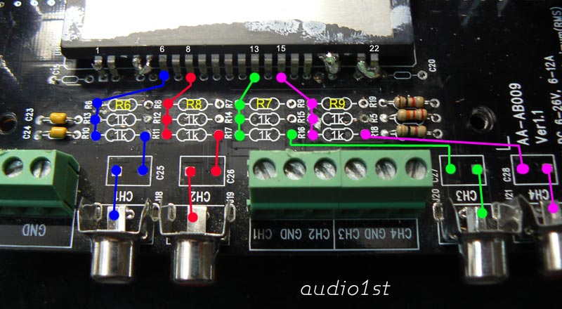
They are pictures of the 4x100 board, I have shown the modified input which shows that the RCA inputs have the better input caps. If you have the updated board it is safe to use the terminal block input.
The other picture shows the 8 resistors that need bridging. they are R11, R19, R26, R33, R39, R47, R54, and R61.
Thanks to Craig for making the effort and the conductive paint is a great idea!
Please note, I do not have one of these boards and all info is based on other peoples findings.
Attachments


Hi guys,
These are some pictures i took of the board before painting the resistors with the conductive paint.
The first is what you can expect to see once you remove the heat sink.
The second is a close up of the resistors which need to be removed or shorted, marked in red. On my board they all had 104 on them. Once these are shorted/removed the trim pots become incredibly sensitive and should allow you to trim out any Offset you may have.
In case any one is wondering, the paint came from Halfords (some time ago!) and is designed to repair the heated rear window circuit in a car, at the time it was the easiest place for me to get conductive paint. I then literally painted the resistors using a fine brush.
Hope this helps,
Craig
Attachments


I confirm that you can adjust the DC offset by bridging the Rs as recommended by Audio1st. I just did mine and the values are now very close to 0. However, I took out all the resisters and bridged them with lead.
Wachara C.
Wachara C.
Last edited:
Hi,
I am Brazlian and I have a doubt. This amplifier can work at bridged mode? Like 2*100 8 ohms.
Sorry my English. Thank's!!!
I am Brazlian and I have a doubt. This amplifier can work at bridged mode? Like 2*100 8 ohms.
Sorry my English. Thank's!!!
Hello everyone, I'm considering getting one of these 4*100W boards off ebay, are there any better sources for them you are aware of? I am located in Australia btw.
I was wondering if it would be possible to use a graphite pencil and just draw a few lines over it, hopefully that will lower its resistance.
Or would it be possible to add a 10K resistor or so in parallel with the old one so the pot adjustment is not too sensitive?
In case any one is wondering, the paint came from Halfords (some time ago!) and is designed to repair the heated rear window circuit in a car, at the time it was the easiest place for me to get conductive paint. I then literally painted the resistors using a fine brush.
I was wondering if it would be possible to use a graphite pencil and just draw a few lines over it, hopefully that will lower its resistance.
Or would it be possible to add a 10K resistor or so in parallel with the old one so the pot adjustment is not too sensitive?
Hi,
I am Brazlian and I have a doubt. This amplifier can work at bridged mode? Like 2*100 8 ohms.
Sorry my English. Thank's!!!
No, these amplifiers are already internally bridged. As such, the channels provided cannot be used in bridged mode.
loleskater, my board arrived quickly less than 10days and im in the UK, also you are buying directly from Sure so i wouldn't worry to much about buying from Ebay.
As for using the graphite pencil, all you can do is try. That was my initial thought as well (from the old days of over-clocking on the PC) but the resistors are very small, and i don't think that would be a particularly permanent solution. But give it a go! the worst that can happen is it doesn't work!
Let us know how you get on.
Craig
I believe Sure will send them from Hefei (near Nanjing) China, straight south to you in Australia.loleskater, my board arrived quickly less than 10days and im in the UK, also you are buying directly from Sure so i wouldn't worry to much about buying from Ebay.
For those wondering, copper-based conductive paint can be bought from Caswell Plating and other electroplating supply places, or you can get the cheaper graphite-based stuff for next to nothing on eBay.
Should I wait 'till the next generation before picking one of these up? Does anyone have any noise/distortion specs?
Should I wait 'till the next generation before picking one of these up? Does anyone have any noise/distortion specs?
Maybe the 100x4 needs to mature.
Hi all.
I have been monitoring this thread for a while and finally have formed an opinion of this amplifier. The gist of the matter is that I have three dead amplifiers. Sure has been gracious in replacing them at no cost but I do not intend to ask for a fourth.
Two of the amps died on power-up, The third lasted about a week around XMAS. During that time, I joined the ranks of those astounded at the quality of the sound the amp produced. I replayed and received new enjoyment from a dozen of my favorite CDs. The amps response seemed tilted toward the bright side just slightly. The party ended when I touched the heatsink to see if it was warm. A puff of smoke and that was that. I took the heatsink off and was surprised to see that three or four pins had been blown off of three of the Tripath devices.
Now since I also purchased the 24v Meanwell supply from Sure, I have opted to buy a 160WX2 module from Class D Audio in California. This is a single supply module which I will try running at 30v for a while. I will revisit the Sure 4x100 (or maybe the 2x100) after a while since the price is attractive. However a brilliant $50 amp must also be reliable as it was jarring to have the music stop so abruptly. I will post a comparison after I get the TAS5615 based module.
JohnG
Hey,
I was wondering if the shorting and offset problems have been fixed with this board?
I'd prefer to not have to send the amplifier back and forwards as things go wrong 😛
Sure's ebay listing says the shorting problem's fixed but confirmation would be great.
Also - untill I get a proper power supply (meanwell 27v) which would be a better choice - a 1.5A 24V power supply or a 19V 5A power supply?
I will not be playing the music too loud but the amplifier surviving is my main priority rather than sound quality?
Thanks
- Status
- Not open for further replies.
- Home
- Amplifiers
- Class D
- Sure Electronics New Tripath Board 4*100W class-D Amplifier Board