non technical questions
After reading the 208 pages I am left with few choices for C9 (and C24) on the other channel:
- Sanyo Oscon 220 μF 35V
- an alternate low ESR 220 μF from another manufacturer.
- 470 μF + 470 μF (non pol) in serie with 0.1 μF film (Wima MKS?) in //
which value should I go for (and why)?
Thank you in advance.
Cheers
Henri
After reading the 208 pages
I am left with few choices for C9 (and C24) on the other channel:- Sanyo Oscon 220 μF 35V
- an alternate low ESR 220 μF from another manufacturer.
- 470 μF + 470 μF (non pol) in serie with 0.1 μF film (Wima MKS?) in //
which value should I go for (and why)?
Thank you in advance.
Cheers
Henri
Re: non technical questions
Henri,
I think either of the last two choices. The Oscon are not designed for coupling, they are an excellent decoupling cap.
Most caps designed for coupling will have copper leads. The others sometimes steel. Use something with copper.
I have only tried several low ESR type here in the feedback loop. I have used Panasonic FM and Rubycon ZL. Both were bypassed with a 0.33 ufd Siemens stacked film and foil naked cap. It seems like the bypassing helped a little.
Once operating, the voltage on this cap is around 0.1 volts. Never tried to measure it on power up and power down. My last one uses a 25 volt rated cap with no issues.
Good luck, you will like it no matter which cap is used.
George
henrik04 said:After reading the 208 pages
- Sanyo Oscon 220 ¼F 35V
- an alternate low ESR 220 ¼F from another manufacturer.
- 470 ¼F + 470 ¼F (non pol) in serie with 0.1 ¼F film (Wima MKS?) in //
which value should I go for (and why)?
Thank you in advance.
Cheers
Henri
Henri,
I think either of the last two choices. The Oscon are not designed for coupling, they are an excellent decoupling cap.
Most caps designed for coupling will have copper leads. The others sometimes steel. Use something with copper.
I have only tried several low ESR type here in the feedback loop. I have used Panasonic FM and Rubycon ZL. Both were bypassed with a 0.33 ufd Siemens stacked film and foil naked cap. It seems like the bypassing helped a little.
Once operating, the voltage on this cap is around 0.1 volts. Never tried to measure it on power up and power down. My last one uses a 25 volt rated cap with no issues.
Good luck, you will like it no matter which cap is used.
George
Re: Re: My new monobloc layout for Mauro Penasa's MyRef Rev. C
Note: This is the 2 side version which Brian and I have produced, but I am working on a single side version which I will make PDFs for and share freely so those who would like to etch it for yourselves can.
My humble opinion:
If you were generating (and sharing) gerber files anyone would be able to use them with local suppliers as it is a standard accepted worldwide. Beside it would let creative minds add change anything they like using software such as Gerbtool (from Wise) or other without being forced to copy / edit graphic files such as .jpg, .png or .pdf
I am thankfull anyway of the efforts that Mauro yourself and Brian have placed in this very original concept.
Henri
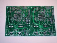
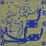
New PCBs in....
Have a look:
PCBs with the 1/4W resistors stuffed. Notice I have the input caps jumpered because I am not using one(no DC from my source). This is also what you would do if you would like to use a large input cap off-board.
Cheers!
Russ
Have a look:
PCBs with the 1/4W resistors stuffed. Notice I have the input caps jumpered because I am not using one(no DC from my source). This is also what you would do if you would like to use a large input cap off-board.
Cheers!
Russ
Attachments
Shipping today
Russ,
Got an email saying the new boards are shipping from Brian. Looking forward to building one of your mono blocks.
For some reason I thought the input coupling cap had to be there. Something like offset voltage on the input and this was maintained by the input cap.
I may be thinking of another circuit. I will remove mine if it works fine without it.
George

Hi,
Good to hear the new boards are about to ship.
I intend to use On Semiconductor MBR 10100 Schottky diodes.
In another thread, t. preferred them to MUR 860 in his My Ref. amp, in his system. He was using his transmission line full range speakers. MUR 860 work very well in his gainclones though.
It seems the MBR 10100 sounded more accurate/balanced in his system. The bass was more defined. Overall detail was improved.
Seems owners of smaller speakers may still prefer the MUR 860, since there is more perceived output in the bass and midrange region, which may be preferred. As t. pointed out, this was just his impressions as heard in his setup. I hope I have reported his observations correctly.
I think t. is an astute listener, so I am interested to see if the MBR 10100 will suit my setup using large fullrange floorstanders.
I only need to swap the boards in my amp, which presently have 25A 400V bridge rectifiers. An easy swap, as they are both Rev C boards.
Audie.
Okay, so, a reverse of direction in the kits.
The CD Silver Mica caps I got are to be too big (body of the cap) and bump into stuff. I will, therefore, revert to the tried and true C0G ceramic caps, but with 5mm pin spacing. Sorry for the false alarms.
I was gonna try different Silver Micas, but there really aren;t many folks making them these days, and I don't like using surplus parts in kits. Anywho...
Kit change
So, I am almost out of the Wima 1.0uF polyesters I have been shipping as input caps. Seems to be fairly universally disliked part, so I am planning to change it.
My current plan is a Solen 1uF 400V MKP axial cap (FastCap). Kit price would remain the same. Thoughts?
It shoulld fit flat on the board in the stanard position.
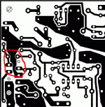
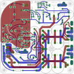
Regarding the final (?) one-sided PCB from the kit...
I downloaded the PDFs.zip from Mauro's thread. Looks pretty nice, but that ground plane is just TOO close to some pads in a few areas. I had to use like 200% zoom just to see whether pads were connected to the ground plane trace or not (especially in the LM3886 area).
Any hope of making it a bit more "legible"?
Khron said:Regarding the final (?) one-sided PCB from the kit...
I downloaded the PDFs.zip from Mauro's thread. Looks pretty nice, but that ground plane is just TOO close to some pads in a few areas. I had to use like 200% zoom just to see whether pads were connected to the ground plane trace or not (especially in the LM3886 area).
Any hope of making it a bit more "legible"?
I have etched more than a few of these with no issues, but I will be glad to take a second look at it.
")
Cheers!
Russ
I'm attaching a snippet of the PCB with the area i'm a bit concerned about.
It's just that, at 100% zoom, the pads over there are clearly touching each other, and i'm almost sure they'll look just like that if i print out the board. Only at 200% zoom is there about 0.5mm of space between that area of the ground plane and the neighbouring pads.
Sorry if i'm a nag, but i really want to build me some RevC's, especially now that i just received my 5-sample order of LM3886s from NatSemicon
edit:
One more questionable area: the same trace, from the inside end of R9 (the middle resistor from the group of 3, above the LM3886) running between the legs of C9 (220uf electro)
Attachments
Hello, i now this is an very old threat, but im searching for PCB's of this monobloc design from russ, maybe is sombody here who have this?
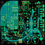
I offer slightly larger PCBs for the MyRef Rev C monoblock, which can use the same BoM as Russ White's v1.2 PCB. The last version of my board is v1.4, which also has component flexibility for various passives, and can accept physically larger (i.e. higher wattage) resistors at many locations (e.g. Philips MRS25 0.6W and PR01 1W resistors in place of some of the 0.25W resistors in the V1.2 PCB). PM or email me at siva dot chander at gmail dot com if you're interested.
Hi there!
I'll do the "thread digger" once again
 !
!
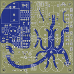
After having the board files from Russ around on my HDD for several years now, I finally managed to get around to them. I've made some minor adjustments to make the boards suit the case and parts that I have around. Probably the biggest change is the resize of the boards to 10x10cm, so I can get them made by dirtypcbs.com. The snap-in capacitors had to go because I'm a little restricted in height - several smaller capacitors fit the bill nicely. Furthermore I've allowed some more space to the resistors, the 220uF feedback cap and the input coupling cap. I've also added a second header for another LED, together with an accompanying resistor, which will get switched off by the relay contact. This way I can use something like a two-color LED which lights up red when the protection circuit kicks in and green when everything is fine.
If anybody is interested and Russ approves, I'll share the gerbers here.
I'll do the "thread digger" once again
!After having the board files from Russ around on my HDD for several years now, I finally managed to get around to them. I've made some minor adjustments to make the boards suit the case and parts that I have around. Probably the biggest change is the resize of the boards to 10x10cm, so I can get them made by dirtypcbs.com. The snap-in capacitors had to go because I'm a little restricted in height - several smaller capacitors fit the bill nicely. Furthermore I've allowed some more space to the resistors, the 220uF feedback cap and the input coupling cap. I've also added a second header for another LED, together with an accompanying resistor, which will get switched off by the relay contact. This way I can use something like a two-color LED which lights up red when the protection circuit kicks in and green when everything is fine.
If anybody is interested and Russ approves, I'll share the gerbers here.
Attachments
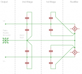
The built in PSU needs sorting.
The first smoothing capacitor must be connected to the rectifier. Use small loop area as your control for trace layout.
Then progress to the second stage of smoothing. Again low loop area controls the trace layout between first and second stage.
Then when the PSU is finished take one trace from Zero Volts to your main audio ground. Alongside that linking trace take the two +ve and -ve supplies and again aim for low loop area.
Do not feed the Speaker Return into the smoothing capacitor junction.
The speaker return must feed into the main audio ground. This "point" becomes the voltage reference for any signal stage that requires that reference.
One final bit of advice:
do not let any trace that passes the PSU charging current share it's part route with any audio signal processing stage.
Last edited:
Thanks Andrew!
I'm still having a somewhat hard time with all this grounding and loop area stuff. I've learned a lot of things about routing which totally makes sense, but the correct way of grounding just won't become second nature to me.
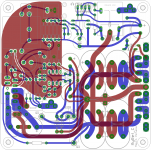
I tried to implement your suggestions in a schematical way first. Please have a look at the two versions and tell me which way would be better. IMHO the second way has less loop area for the first smoothing stage, but I'm not too sure about what to do with the second stage or where to merge the "upper ground" and the "lower ground" together. The separation into stages seems to force the introduction of several intermediate ground points, like in the first scheme. I could have added another one right between the rectifiers, but that didn't seem to be such a good idea.
What about returning every single capacitor to this central point between the rectifiers and then running a single trace from there to the main audio ground? That would look pretty much like what I did above in the actual layout (except for the separate main audio ground), but wouldn't show any distinct stages anymore. Loop area for every single cap should be minimized, however.
I'm still having a somewhat hard time with all this grounding and loop area stuff. I've learned a lot of things about routing which totally makes sense, but the correct way of grounding just won't become second nature to me
.I tried to implement your suggestions in a schematical way first. Please have a look at the two versions and tell me which way would be better. IMHO the second way has less loop area for the first smoothing stage, but I'm not too sure about what to do with the second stage or where to merge the "upper ground" and the "lower ground" together. The separation into stages seems to force the introduction of several intermediate ground points, like in the first scheme. I could have added another one right between the rectifiers, but that didn't seem to be such a good idea
.What about returning every single capacitor to this central point between the rectifiers and then running a single trace from there to the main audio ground? That would look pretty much like what I did above in the actual layout (except for the separate main audio ground), but wouldn't show any distinct stages anymore. Loop area for every single cap should be minimized, however.
Attachments
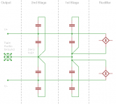
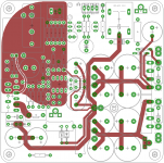
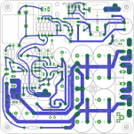
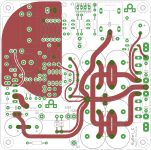
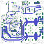
Here's another try. Needs some tidying, but first of all it has to be OK. I've attached images of the separate layers for better visibility.
What would you say? Is this better? What else should be done?
What would you say? Is this better? What else should be done?
Attachments
- Status
- This old topic is closed. If you want to reopen this topic, contact a moderator using the "Report Post" button.
- Home
- Amplifiers
- Chip Amps
- My new monobloc layout for Mauro Penasa's MyRef Rev. C