Your first batch of PCBs probably costs similar to the BOM for a single channel of MyRef. So I would just trash it.
If I were you I would not hurry with the second layout. Take your time, try different strategies, may be even change the layout drastically. Attached is the idea of an easier to route layout which would also be easier to place inside of narrow chassis along the heatsink.
If I were you I would not hurry with the second layout. Take your time, try different strategies, may be even change the layout drastically. Attached is the idea of an easier to route layout which would also be easier to place inside of narrow chassis along the heatsink.
Attachments
I would just trash it.
Do you really think it's that bad?
 I think we're talking about marginal improvements here (right next to the "point of diminishing returns"), and not about crap vs. useable...
 IIRC Russ pointed out that he placed the relay as far away from the LM3886 as possible for a reason. Don't remember what it was exactly, but it must have had some detrimental effect if the relay was placed close to the IC.
If at some moment I get to know that the design I use is not optimal I feel the need to improve it
If that's all... I can live with you losing sleep over my layout!
I jused to think just like that. One day I realised that this kept most of my projects in the development stage, because I kept refining or changing things with no end. I finally learned to just be content at some point in time and just build that thing. With that "prototype" running I would then decide to keep it, refine it or toss it. Of course this would not be necessary if I knew beforehand how to do everything 100% right, but this is certainly not the case most of the time
.If the relay coil is fed with non changing DC, then there is no effect to be taken into account.
What do you consider "non changing DC"? With the proposed circuit we're talking about 19.5VDC with a ripple of ~250mVPP.
If that's all... I can live with you losing sleep over my layout!
I jused to think just like that. One day I realised that this kept most of my projects in the development stage, because I kept refining or changing things with no end. I finally learned to just be content at some point in time and just build that thing. With that "prototype" running I would then decide to keep it, refine it or toss it. Of course this would not be necessary if I knew beforehand how to do everything 100% right, but this is certainly not the case most of the time
I totally agree with you on all this. I have several half done/partially working projects at hands
But at the same time I have a lot of fun this way. If all is finished one day then there will be nothing else to doWhat do you consider "non changing DC"? With the proposed circuit we're talking about 19.5VDC with a ripple of ~250mVPP.
If such amount of ripple across the relay coil can magnetically couple to the signal then you can use a regulator to feed the coil.
Which I do all the time.If such amount of ripple across the relay coil can magnetically couple to the signal then you can use a regulator to feed the coil.
Run a 12V relay from 15V to 18V regulated supply with a current saving resistor to reduce dissipation when "always ON".
For the best performance, you need the reference/input ground to connect to the power ground at the speaker output ground connection. You can read my rationale for this, as well as see the simulations I use to back up this claim, on my Taming the LM3886 pages. You'll note that AndrewT makes the same recommendation ad nauseam.
Secondly, use the available copper. The board fab charges the same whether you use the copper or not, so I really don't get the idea behind the complicated pour shapes and snaky traces. This goes both for the supply routing and the ground routing. The layout shown in Post #55 gets one of these right.
Number of layers: I don't see a need for a 5-layer board as mentioned earlier in this thread. I am getting world class performance with a well-designed 2-layer board on the Modulus-86. The cost riser from two layers to four or six is large. For a once off run through a cheapie manufacturing outfit going with a 6-layer board may be OK for DIY purposes, but it's not always a wise decision from a business/production/technical standpoint. Tradeoffs, tradeoffs.
Regarding magnetic coupling through relays, I suggest reading some relay data sheets. Pick a relay with good isolation between the coil and the contacts. Alternatively, pick a relay and measure the coupling. This is trivial to do with a computer sound card and some software like TrueRTA. I bet you'll find that it is very, very hard to couple anything into the output node of the amp at the frequencies relevant to ripple (48 Hz to a few kHz).
Tom
Last edited:
If all is finished one day then there will be nothing else to do
True, but what if you actually need such a thing you're planning, or want to use it on a daily basis to finally supersede a years-old makeshift solution? Building things for fun is fun, but sometimes you (or I, at least) actually need such a thing...
Which I do all the time.
Run a 12V relay from 15V to 18V regulated supply with a current saving resistor to reduce dissipation when "always ON".
I'll consider this for the routing-remake V.2 TM.
For the best performance, you need the reference/input ground to connect to the power ground at the speaker output ground connection.
Yeah, but how shall I do that? Obviously I can't put all those parts physically into the same space, so there has to be some copper in between. Okay, one point is to move the relay closer to the IC to shorten that track. What about the layout from post #60? Is that better already than that from #55? What if input ground plane and output ground plane were put together as one plane and connect to the power ground plane at one point? I've read all your suggestions several times now, but it still leaves me with some uncertainty.
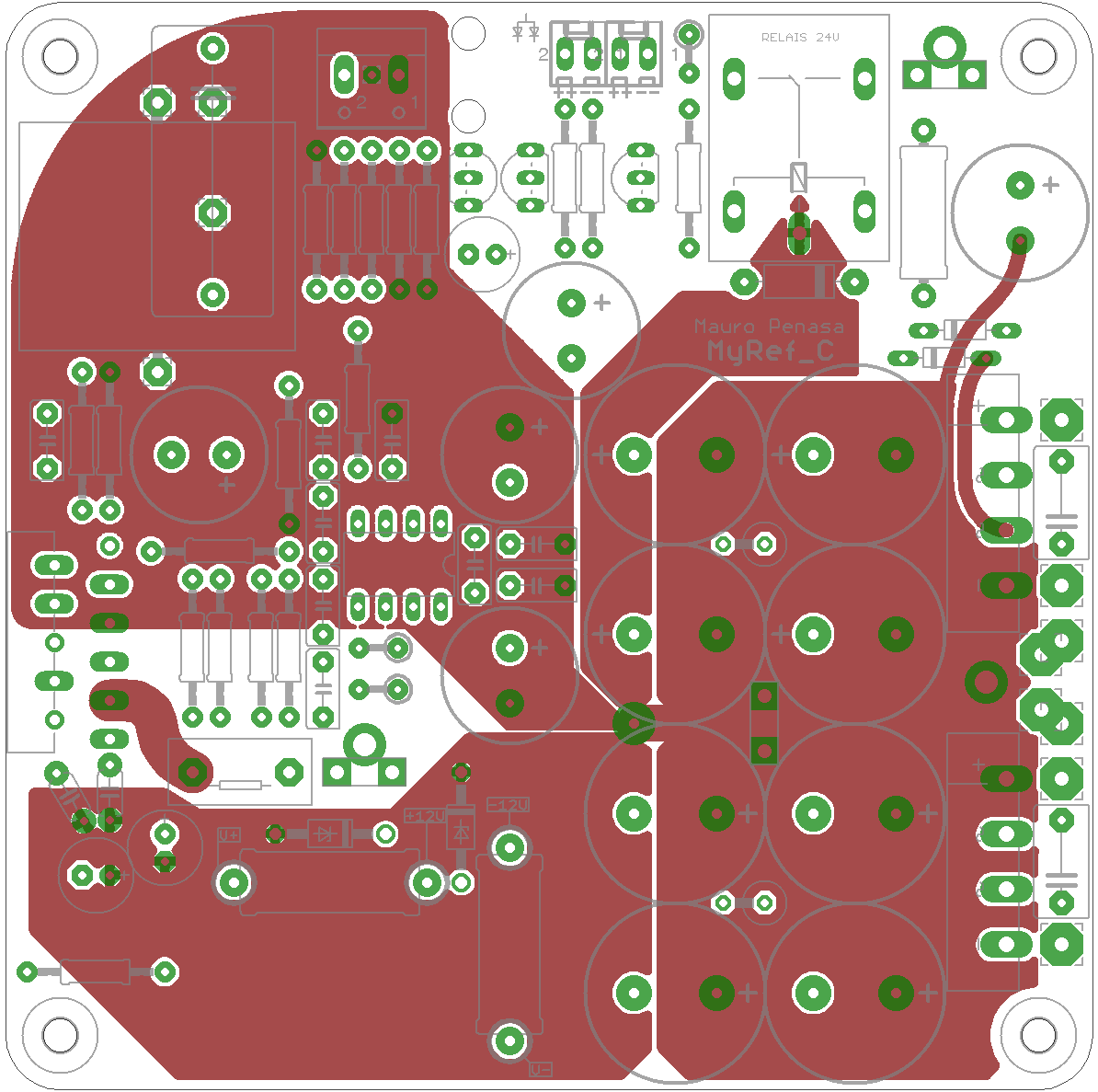
I tried to resemble Tom's simulations with the MyRef-schematic and generic models in LTspice. The only thing that really makes a difference is connecting GND_SIG directly to GND_SPK, just like his website proposes. Thus it seems best to include the speaker relay pin into the signal ground pour and then route a trace from that same relay pin to the power ground. The star ground that I've laid out on the fabricated boards simulates rather bad in comparison .
.For the best performance, you need the reference/input ground to connect to the power ground at the speaker output ground connection.
So to apply this to any amplifier you would just not hook up the signal ground to the pcb signal in(to prevent ground loop), and instead run it to the speaker negative terminal?
Just using a naked wire? Or shielded with non-speaker end grounded and speaker end not?
Thanks
No. The signal input is two wires and both wires must remain close coupled all the way from input socket to PCB input pads. Both wires, even if coaxial need to be connected at both ends.So to apply this to any amplifier you would just not hook up the signal ground to the pcb signal in(to prevent ground loop), and instead run it to the speaker negative terminal?
Certainly not naked wire. All inter-module signal connections are two wire, connected at both ends.Just using a naked wire? Or shielded with non-speaker end grounded and speaker end not?
Thanks
Balanced impedance connections require two signal wires that are connected at both ends to impedances that are as close to identical as possible, generaly better than 0.1% for resistance matching and better than 1% for capacitance matching.Also: Just realized that to avoid ground loops I will make cables that are open at the amplifier's XLR pin 1. So there is no ground to be routed... Advice?
These signal wires are connected to pin2 for "hot" and pin3 for "cold".
Pin1 is for screen/shield and is ALWAYS connected to Chassis.
No. The signal input is two wires and both wires must remain close coupled all the way from input socket to PCB input pads.
So the PCB itself has to be designed so that the input ground already goes to speaker ground. In other words, don't try to adapt an already made amplifier to run IN Gnd to SPKR Gnd?
The input signal return may not be connected to the speaker output return.So the PCB itself has to be designed so that the input ground already goes to speaker ground. In other words, don't try to adapt an already made amplifier to run IN Gnd to SPKR Gnd?
You need to check that.
The amplifier works like an opamp.
The opamp does not need a ground. The output signal is a scaled version of the DIFFERENCE between the two input signals.
But the output signal has to have a reference to be able to use that output voltage.
The reference is back to the Input. Same as an opamp.
This reference connection is usually on the PCB, but not always.
Sometimes it is a direct trace connection. This works well for a monoblock, but not for a dual mono, nor a stereo build.
Sometimes it is a resistance connection. This is the HBRR & HBRL that D.Joffe talks about.
Sometimes it is a LONG trace with very high impedance. This is bad.
Sometimes it needs an off board connection. If this off board connection includes a big loop area, then this will pick up interference. This is bad, worse than the LONG trace version. Do not take an off board reference connection away to some remote point to then be brought back from that remote point to the other end of the referenced circuit.
Last edited:
- Status
- This old topic is closed. If you want to reopen this topic, contact a moderator using the "Report Post" button.
- Home
- Amplifiers
- Chip Amps
- My new monobloc layout for Mauro Penasa's MyRef Rev. C