Hi Metal,
That's cool. BTW, I agree on the cap inside the coil thing when talking about crossovers. The heat alone would cause troubles for the cap. I would predict an early failure of the cap.
Coil around the resistor for this particular circuit is not normally a problem. You're right, it's a convenience thing and a space saver. Why not then?
-Chris")
That's cool. BTW, I agree on the cap inside the coil thing when talking about crossovers. The heat alone would cause troubles for the cap. I would predict an early failure of the cap.
Coil around the resistor for this particular circuit is not normally a problem. You're right, it's a convenience thing and a space saver. Why not then?
-Chris
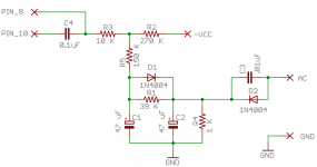
Yeah! Right from the onset I had my doubts regarding the winding around the resistor as field through the inductor and resistor reaction giving complexities. I have decided the standalone inductors and got 3 µH inductors wound according to the metrics obtained from the following online inductor calculator!
Barry's Inductor Simulation
It is 10mm in diameter.
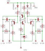
My project is to swap the [ii] version with [v] for better THD. They are already functional with STK 4192ii circuits given above. The PCBs are really tiny and I now face the problem of placing the inductors. So I used spacers to elevate the Zobel and snubber from the PCB. But I am unhappy as inductor fields might have some adverse effects on the capacitors below.
How far should be the inductors away from the capacitors?
I can implement the Zobel and snubber totally away from the main PCB as it is built on a vero board now! But long trace before the Zobel and snubber might give oscillation to IC?
Till I build new PCBs for 4191V I will have to be satisfied with this configuration. Can you see some problems in it?
Barry's Inductor Simulation
It is 10mm in diameter.
My project is to swap the [ii] version with [v] for better THD. They are already functional with STK 4192ii circuits given above. The PCBs are really tiny and I now face the problem of placing the inductors. So I used spacers to elevate the Zobel and snubber from the PCB. But I am unhappy as inductor fields might have some adverse effects on the capacitors below.
How far should be the inductors away from the capacitors?
I can implement the Zobel and snubber totally away from the main PCB as it is built on a vero board now! But long trace before the Zobel and snubber might give oscillation to IC?
Till I build new PCBs for 4191V I will have to be satisfied with this configuration. Can you see some problems in it?
Hi Chris,
TKs for the advice!!
That sums it up I suppose! I am sort of a guy who is a perfectionist! We all are for that matter being DIYAudio members!
I will wire the amp amd see how it goes and let know the results. BTW I have made new Elliot 98 preamp on the veroboard and already using STK mute circuit for the good effect. Need to buid the protection circuit too.
Attachments
- Status
- This old topic is closed. If you want to reopen this topic, contact a moderator using the "Report Post" button.