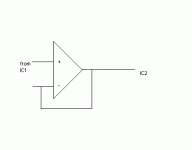
The gain of IC1 is set by the two resistors (and pot), you have made the gain variable to adjust the Q of the filter. You have taken the output from the feedback node here because if you use the actual output of the op-amp you get a change in gain (level) as the Q is adjusted.
Your error is that you have driven the next filter stage (IC2) from the junction of these resistors. This has 2 bad effects:
1. The next filter stage (IC2) will have it's response messed up because it is not being driven from a low impedance source. It is being driven by a source impedance equal to the parallel combination of the upper and lower legs of the IC1 feedback network.
2. The next filter stage (IC2) input impedance is in parallel with the lower leg of the IC1 feedback network, hence the gain will not be as predicted, and there may even be errors introduced by some of the IC2 signal finding its way back into the feedback network of IC1, thus causing instability or distortion.
To solve these problems you need to add a buffer. All you need to do is add another op-amp driven from IC1 feedback node, then use this to drive IC2 filter.
i understod it like this sorry for image quality (paint).
If i chance LP as well variable should it have too buffer?.
I guess it should.
What do you think using polyphenylene sulphide capasitors in filter? (http://www.farnell.com/datasheets/27371.pdf)
If i chance LP as well variable should it have too buffer?.
I guess it should.
What do you think using polyphenylene sulphide capasitors in filter? (http://www.farnell.com/datasheets/27371.pdf)
Attachments
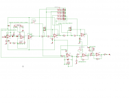
Your diagram is correct.
Yes, everytime you want to drive another circuit from the same point as the feedback node, you need a buffer to stop the feedback getting spoilt and to ensure the following circuit is driven properly. However, I'm not sure that you would gain much from making the lowpass filter adjustable Q. Linkwitz-Riley takes some beating") Even if your main speakers don't roll off quite at the same Q/slope, it will be hard to tell. And you add an extra couple of op-amps doing it.
Even if your main speakers don't roll off quite at the same Q/slope, it will be hard to tell. And you add an extra couple of op-amps doing it.
Yes, everytime you want to drive another circuit from the same point as the feedback node, you need a buffer to stop the feedback getting spoilt and to ensure the following circuit is driven properly. However, I'm not sure that you would gain much from making the lowpass filter adjustable Q. Linkwitz-Riley takes some beating
Even if your main speakers don't roll off quite at the same Q/slope, it will be hard to tell. And you add an extra couple of op-amps doing it.I made my lowpass variable because then I can change my main speakers without messing with the sub internals. However, I had to use 2 dual gang pots as it's hard to find 4 gang ones, which is a bit of a pain. Also, you get more error by adding a pot as they are not very accurate/well matched between gangs.
Looking good
I think you need to look at the last part of your circuit with the level adj and phase. Firstly, I'm confused why you have a second level adjustment, and the way it's implemented being fed from S1 and IC2B doesn't look right to me. I'm guessing you are trying to make a bypass. You need to make the output buffer choose between filter or not.
Your phase switch doesn't look right to me either, and because the is no DC bias path for the non-inverting input of IC4B it will go mad when you flick the switch.
I found the phase turn schema on there
http://sound.westhost.com/project103.htm
They explain there why 2 stage.
(not sure why)
Do i need a buffer again on bypass of the filters.
(first is DC protection.)
http://sound.westhost.com/project103.htm
They explain there why 2 stage.
(not sure why)
Do i need a buffer again on bypass of the filters.
(first is DC protection.)
If you look at the schematic on the ESP site again, you will see that the non-inverting input is always connected to ground via the resistors. The way you have it is not the same as ESP.
On the other problem, you don't need any more buffers, you just need to change your circuit slightly. What you need is to have the switch connected to your output (after the 50 ohm resistor) and it selects between the output from IC1A (for bypass) and the output of the filter+phase shift.
On the other problem, you don't need any more buffers, you just need to change your circuit slightly. What you need is to have the switch connected to your output (after the 50 ohm resistor) and it selects between the output from IC1A (for bypass) and the output of the filter+phase shift.
The schematic in your 22 November post looks fine. I'm not sure what you are trying to do with your other schematic in the 'for bridged amp' part. I think it's wrong. If you want to make a signal to drive a stereo amp in a bridge way, all you need is an inverted copy of the original signal.
Note that you ABSOLUTELY MUST use a single/shared PSU for the amps if you want to bridge it . You CANNOT use dual mono configuration.
If you are going to have a gain control on your controller it would be better right after the input buffer. I would actually just make the input buffer the gain control and take the feed for the bypass connection directly from the input before the buffer.
Thanks for comments again.
gain is the same as in earlier schema mute to +9db volume control.in fact the hole schema is same exept U9 and U10 and components around them
i changed end of schema because i need both bridged and normal output.( 3 out connectors (normal+ and bridge + and bridge-))
forget the gound and 100k resistors at the end of schema they are there because of simulation program (circuitmaker).
Schema worked fine on program but i wanted other opinions.
I used U9 and U10 to make first 180 degree turn and then another 180 degree turn.
2 stage because i have only opa2134 and there will be problems if you dont use both amplifiers in dual amp.
Please check it and correct if i`m wrong in soimething.
Cheers jyri
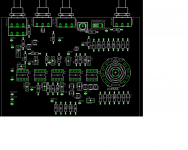
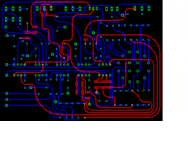
Added circuitboard for schematic.
Could you guyes check how horible it is.
Capasitors are SMD polyphenylene sulphide from panasonic
i`v heard that they are best for audio use.
grounding is starground (think so)
CB looks pretty horible but could you guys check is there massive mistakes which i should repair.
This is my first one.
Could you guyes check how horible it is.
Capasitors are SMD polyphenylene sulphide from panasonic
i`v heard that they are best for audio use.
grounding is starground (think so)
CB looks pretty horible but could you guys check is there massive mistakes which i should repair.
This is my first one.
Attachments
- Status
- This old topic is closed. If you want to reopen this topic, contact a moderator using the "Report Post" button.
- Home
- Amplifiers
- Chip Amps
- active filter