Are you using separate supplies? If not, implement the "hum loop break resistors" between input gnd and power gnd as described here http://www.updatemydynaco.com/documents/GroundingProblemsRev1p4.pdf page 4 onwards
Yes, but this frequency is too high in my opinion. TDA2030 and similar uses caps in the order of 10 nF, one thousand higher.
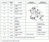
Are those R5 & C8 in the TDA2030 data sheet? Also what do you think would be an appropriate frequency for this part of the circuit?
Thanks.
Are you using separate supplies? If not, implement the "hum loop break resistors" between input gnd and power gnd as described here http://www.updatemydynaco.com/documents/GroundingProblemsRev1p4.pdf page 4 onwards
Sorry if I'm being thick - what do you mean by separate supplies?
The same resistors are shown in Bonsai's doc, but there is a bit more of an explanation about how they work in Joffe's. Andrew T mentioned them too, with reverse parallel diodes across them as an added precaution incase they fail, failure potentially causing the negative rail to be seen across the output (I think?)
Last edited:
Read TomChr for an explanation of how to avoid oscillation when connecting a capacitor to the -IN node. There are a few articles explaining opamp stability where this upper leg NFB capacitor is used.Are those R5 & C8 in the TDA2030 data sheet? Also what do you think would be an appropriate frequency for this part of the circuit?
Thanks.
When you use this capacitor, it provides a route for interference at the speaker leads to be injected direct into the -IN input. You MUST do something to attenuate that interference.
Read D.Joffe. HBRR & HBRL are needed for every multi-channel amplifier where the Source component combines the Signal Returns at the source.
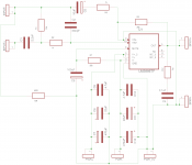
Thanks for all the input, I've read and re-read the links you provided me and have updated the schematic and drafted a layout. After reading the stability guidance on neurochrome.com I've revised the schematic. Hopefully I'm moving forward, here are the new designs:
Any feedback much appreciated, thanks.
Any feedback much appreciated, thanks.
Attachments
Thanks for looking, I added this following comment in post #9
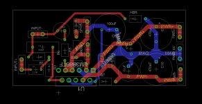
When I added that trace, it created a link to 0v - should I have done that a different way?
You will need to add a voltage reference between Signal return and speaker return so that the "amp" can work out what voltage it needs on the speaker output.
This extra voltage reference link can be a copper trace. It needs to meet the siganl return trace at a point and it needs to meet the speaker return trace at a point.(MAG)
When I added that trace, it created a link to 0v - should I have done that a different way?
The value of C5 looks too low. Did you follow Tom's guidelines on calculating the values of parts around LM3886?
On your PCB layout the PWR- trace touches the PWR+ (pin 1 of the LM38886), PWR+ touches MAG at the "+" pin of C7. You also use some random footprints for the parts, e.g. your 2u2 input cap is much smaller in size than 680p cap. The footprint of C6 is also a bit too large. Did you check what are the typical sizes of various parts? I would recommend to decide on the BOM (using standard industrial parts) and then start laying out the PCB. Also add mounting holes and use proper connectors for the input. You definitely do not want to use fast-on connectors for it.
Regards,
Oleg
Last edited:
Since you are designing two layer PCB then turn one layer into the GND plane. Then move the power traces to the same side of the PCB above the GND plane. Make power/output GND plane separate from input/feedback GND plane and connect them at the output terminal as Tomchr suggests. Use HBRR/HBRL resistors for this if you plan a stereo setup.
Comments on the layout:
HBR should connect spkr- to input-. Try to see HBR as an extra resistor in the feedback loop.
Use a plane for power/speaker ground.
Place spkr- near C9/C12. This will ensure the lowest path for HF current.
Place C9/C12 so that the ground connections are close together.
Use a plane for input-. This way you can keep the loops small.
The value of C5 looks too low. Did you follow Tom's guidelines on calculating the values of parts around LM3886?
On your PCB layout the PWR- trace touches the PWR+ (pin 1 of the LM38886), PWR+ touches MAG at the "+" pin of C7. You also use some random footprints for the parts, e.g. your 2u2 input cap is much smaller in size than 680p cap. The footprint of C6 is also a bit too large. Did you check what are the typical sizes of various parts? I would recommend to decide on the BOM (using standard industrial parts) and then start laying out the PCB. Also add mounting holes and use proper connectors for the input. You definitely do not want to use fast-on connectors for it.
Regards,
Oleg
Thanks Oleg, C5 was a mistake - I calculate this to be 220uF - does that sound more sensible? When you talk about Tom's guidelines, are they the ones here or is there some additional guidance that I've not yet found?
I'm maintaining a BOM alongside the schematic and the footprints are taken from the datasheets: C6 is a Nichicon KZ 100v 100uF; the 2u2 cap is a Wima polyester and the 680pF cap is a Silver Mica. Perhaps I've chosen the wrong types of caps - do they seem like sensible choices?
One final question, what type of connections would you suggest instead of faston?
Thanks,
Simon.
Yes, the link to Tom's guidelines is the correct one. I am not aware of the other.
Input connector can be 2.54mm pitch molex or 5.08mm pitch screw terminal. Depends on your preference.
As for the capacitors choice I guess for 680p a part with smaller footprint can be found since it only sees signal input level voltage.
Input connector can be 2.54mm pitch molex or 5.08mm pitch screw terminal. Depends on your preference.
As for the capacitors choice I guess for 680p a part with smaller footprint can be found since it only sees signal input level voltage.
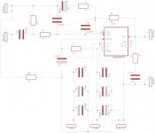
Thanks for all your comments, I've updated the schematic and layout - does this look as though I'm going along the right lines now? I've left the components as they were for now, if the circuit looks okay I'll review the BOM.
Regards,
Simon.
Regards,
Simon.
Attachments
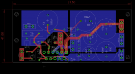
The schematic is correct re inverting input connection and HBR. On the PCB layout the two input terminals are too far apart and the power supply decoupling capacitors should be as close to the chip as possible, I'd suggest 100nF and 100uF, the smaller value closest to the chip
- Status
- This old topic is closed. If you want to reopen this topic, contact a moderator using the "Report Post" button.
- Home
- Amplifiers
- Chip Amps
- Newbie LM3886 Circuit