I don't believe currents flow in lines. I also don't believe currents leave the plane at the edges. Just an example of the spread of flow.
"current follows the path of least resistance" I have read this in several places put it cant be true, Current flows though all paths relative to the resistance. It does not only follow the path of least resistance.
My first example is somewhat exaggerating the spread of the flow and takes no consideration of the supply traces.
Let's change the word "resistance" to the word "impedance". The higher the frequency the less obvious the impedance of any path will be. The big player will be self-inductance.
I don't believe currents flow in lines.
Unless you're referring to eddy currents, electrical current flow is a laminar flow as far as I know.
I also don't believe currents leave the plane at the edges.
Of course the current doesn't leave the plane at the edge. If you're referring to the colorful figure I posted yesterday, it's half the current flow. The path is symmetric so half is modeled and shown. This allows you to see the 3D current density distribution on a 2D screen. The other half is identical.
"current follows the path of least resistance" I have read this in several places put it cant be true, Current flows though all paths relative to the resistance. It does not only follow the path of least resistance.
Of course, the current doesn't just pick the mathematical line of least resistance and only flow there. Think of the ground plane as an infinite number of resistances in parallel. The lowest resistance will be that of the direct path from point A to point B along the surface of the plane. That will have the highest current density (red in the colorful picture from yesterday). Now imagine the current that flows from point A at the top of the plane, down to the bottom of the plane, then along the bottom surface, and up to the top of the plane by point B. That route will have slightly higher resistance as it travels a longer distance through the plane (finite conductance). This route will have slightly lower current density. Now consider the route that goes from point A, along the surface of the plane to the edge of the plane, then along the edge until it jogs in and hits point B. That route is much, much, much, much longer hence it'll see a much, much, much, much lower current density (blue in the colorful picture I posted last night). Now you repeat this exercise for the infinite number of routes in the plane and you'll end up with the same colorful picture. The current density is the highest in the direct path between point A and B and decays exponentially as you move away from the direct path.
You can also look at the electric field. The field goes from + to -, hence it starts at the trace and terminates at the ground plane. I dug up this example. It's a micro-strip antenna, but the only difference between a "trace" and an "antenna" is really the marketing. An "antenna" is just a "trace" that's been optimized to a specific radiation pattern.
The highest current density will be where the EM field line density is the highest (i.e. many lines bunched together --> high current density).
An externally hosted image should be here but it was not working when we last tested it.
If this doesn't drive the point home, then I suggest consulting an electromagnetics text or semiconductor physics text. Streetman is a common undergraduate text for semiconductor physics.
I'll go build circuits now.
~Tom
My comment on currents leaving the plane at the edges was directed at my own post. My limited attempt at showing DC currents on a plane.
I found this one, it contains some good examples in the audio bandwidth.
http://pdfserv.maximintegrated.com/en/an/TUT5450.pdf
I found this one, it contains some good examples in the audio bandwidth.
http://pdfserv.maximintegrated.com/en/an/TUT5450.pdf
That's no surprise to me. It was, however, surprising to see the current density change already at 50 kHz. That's pretty damn close to DC in my opinion... I don't doubt the results, though.
Anyway... Mucked some more with the layout. Stare at attached.
There are two main changes:
1) The Zobel network got rearranged such that the Zobel ground moved a lot closer to the HF ground by the decoupling caps. Also, I found a 100 nF C0G/NP0 ceramic cap(!). That should work just fine.
2) The decoupling caps moved closer to the LM3886. One of them was rotated to move its ground pin closer to the HF ground.
To address KSTR's concern: The fringe cap between the VCC and the OUT pours will be swamped by the cap to the ground plane. So I'm not so concerned with the proximity of the pours. If it turns out I'm wrong, I can easily change the pours with a Dremmel...") The joy of prototypes.
The joy of prototypes.
I ended up taking the small signal ground for the op-amp circuitry south of what's shown in the image by the output connector. As KSTR pointed to, that's probably going to be the quietest spot in the plane.
The board goes in the ferric chloride soup tomorrow. I'll keep you posted.
~Tom
Anyway... Mucked some more with the layout. Stare at attached.
There are two main changes:
1) The Zobel network got rearranged such that the Zobel ground moved a lot closer to the HF ground by the decoupling caps. Also, I found a 100 nF C0G/NP0 ceramic cap(!). That should work just fine.
2) The decoupling caps moved closer to the LM3886. One of them was rotated to move its ground pin closer to the HF ground.
To address KSTR's concern: The fringe cap between the VCC and the OUT pours will be swamped by the cap to the ground plane. So I'm not so concerned with the proximity of the pours. If it turns out I'm wrong, I can easily change the pours with a Dremmel...
The joy of prototypes.I ended up taking the small signal ground for the op-amp circuitry south of what's shown in the image by the output connector. As KSTR pointed to, that's probably going to be the quietest spot in the plane.
The board goes in the ferric chloride soup tomorrow. I'll keep you posted.
~Tom
Attachments
Finally... I managed to get the PCB optimized. See attached.
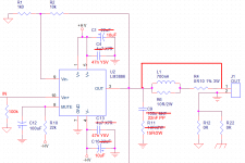
KSTR has previously expressed some concern about the VCC and OUT pours running side-by-side. The currents in the VCC pour are not pretty. The LM3886 is a class AB amp, after all. However, the VCC pour is tightly coupled to the ground plane on the bottom layer. Hence, I strongly suspect that the nastiness will couple to the ground plane through the sizable plate capacitance, rather than cross to the OUT pour via the much lower fringe capacitance. Also, the OUT node is of rather low impedance (probably a few ohm, open loop).
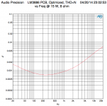
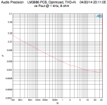
I've included the THD vs frequency for Pout = 15 W, 8 Ω and for THD vs Power at 1 kHz, 8 Ω.
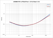
Now the moment we've all been waiting for: Which is better, PCB or P2P?
Sorry to disappoint, but there is no clear winner. The two are line-on-line through most of the audio spectrum. In the low end, there's a slight discrepancy due to measurement tolerances and repeatability. In the high end, there's a slight difference in favor of the PCB - probably due to the use of lower inductance planes rather than wires.
The bottom line is that a poor layout will lead to poor performance - regardless of P2P or PCB. A good layout requires real work.
Note that I'm using the same components as I did for the P2P experiment. The Zobel needs optimization and the bypassing needs improvement as I've noted elsewhere. Optimizing the Zobel should have no impact on the THD. Optimizing the bypassing might improve THD, though, it most likely will not. Both will improve stability with capacitive load, but that's another story.
~Tom
KSTR has previously expressed some concern about the VCC and OUT pours running side-by-side. The currents in the VCC pour are not pretty. The LM3886 is a class AB amp, after all. However, the VCC pour is tightly coupled to the ground plane on the bottom layer. Hence, I strongly suspect that the nastiness will couple to the ground plane through the sizable plate capacitance, rather than cross to the OUT pour via the much lower fringe capacitance. Also, the OUT node is of rather low impedance (probably a few ohm, open loop).
I've included the THD vs frequency for Pout = 15 W, 8 Ω and for THD vs Power at 1 kHz, 8 Ω.
Now the moment we've all been waiting for: Which is better, PCB or P2P?
Sorry to disappoint, but there is no clear winner. The two are line-on-line through most of the audio spectrum. In the low end, there's a slight discrepancy due to measurement tolerances and repeatability. In the high end, there's a slight difference in favor of the PCB - probably due to the use of lower inductance planes rather than wires.
The bottom line is that a poor layout will lead to poor performance - regardless of P2P or PCB. A good layout requires real work.
Note that I'm using the same components as I did for the P2P experiment. The Zobel needs optimization and the bypassing needs improvement as I've noted elsewhere. Optimizing the Zobel should have no impact on the THD. Optimizing the bypassing might improve THD, though, it most likely will not. Both will improve stability with capacitive load, but that's another story.
~Tom
Attachments
-
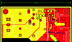
 LM3886_PCB_R2p0_ALL.png88.9 KB · Views: 1,207
 -
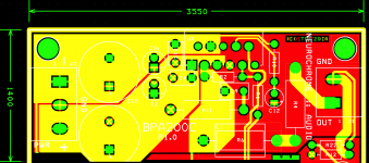
 LM3886_PCB_R2p0_TOP.png84.7 KB · Views: 1,153
 -
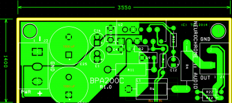
 Screen Shot 2014-04-21 at 12.10.03 AM.png54.9 KB · Views: 1,118
 -
 Screen Shot 2014-04-21 at 12.24.48 AM.png60.1 KB · Views: 393
 -
 LM3886_P2P_vs_PCB.png98.3 KB · Views: 439
 -
 LM3886_PCB_R2p0_Schematic.png45.6 KB · Views: 761
Last edited:
a good primer for current flow...
http://www.x2y.com/filters/TechDay0...log_Designs_Demand_GoodPCBLayouts _JohnWu.pdf
One of the problems with protective earth (grounded) equipment and interconnects with braided screens is the low frequency audio will travel round the ground connections as they are often a lower resistance path than the braided screen on the IC.
Most low level and sensitive analogue designs (not all audio, mainly instrumentation) have ground planes and power planes, this allows much better control of impedances and allows better power supply integrity, it also provides better protection from EMI. Where power outputs are required the high power sections will be split and the ground separated to avoid the high current swamping the low level signals.
A good PDF, it is nice to see information about how critical and what decoupling caps do (provide power).
Nice to see a layout with some decent grounding
Nice to see a layout with some decent grounding
Thanks! Also note the low-inductance power feeds and decoupling. That's where the majority of the layout time was spent, actually.
~Tom
Mmm, that depends. 95% braids are usually around 41x40, which is actually a little lower resistance than the AWG 16 commonly found in power cords (3.8 versus 4 mOhm/foot in this example). It's also routine to have multiple interconnects in parallel but uncommon to have multiple power cords (outside of several kW pro audio installations). So it's often the case ground offsets between audio components in decent installations are limited by interconnect shield impedance. Which, since resistances are low, is typically inductive from around 1kHz up. Give or take, oh, a factor of two to a hundred depending on the installation. With home/DIY audio usually being at the low end of that range.low frequency audio will travel round the ground connections as they are often a lower resistance path than the braided screen on the interconnect
Yeah, noise management in power amps often looks rather like mixed signal design, albeit with greater emphasis on in band rejection through regulation than out of band rejection with passive filters. However, a more useful current flow reference for audio is probably star of stars along with the notion of distinguishing between ground_safety, ground_power, and ground_signal. I actually figured out a somewhat more refined version of that article independently and then came across it later. Applying stuff one tends to worry about up in the MHz or GHz range to kHz circuits is certainly valuable for high precision but looking at DIYA's articles section yielded a rather d'oh sort of moment all the same.Where power outputs are required the high power sections will be split and the ground separated to avoid the high current swamping the low level signals.
Mmm, that depends. 95% braids are usually around 41x40, which is actually a little lower resistance than the AWG 16 commonly found in power cords (3.8 versus 4 mOhm/foot in this example). It's also routine to have multiple interconnects in parallel but uncommon to have multiple power cords (outside of several kW pro audio installations). So it's often the case ground offsets between audio components in decent installations are limited by interconnect shield impedance. Which, since resistances are low, is typically inductive from around 1kHz up. Give or take, oh, a factor of two to a hundred depending on the installation. With home/DIY audio usually being at the low end of that range.
Between a pre-amp and power amp you generally have one interconnect, both power amp and pre-amp are plugged into the mains pretty close...Jneutron did some maths and illustration on his gallery regarding this. It is not always the case but is one of the unseen (by many) problems that may arise, more often when bespoke esoteric cables are used.
Found it FYI:
http://www.diyaudio.com/forums/gallery/showphoto.php/photo/9530
Yeah, noise management in power amps often looks rather like mixed signal design, albeit with greater emphasis on in band rejection through regulation than out of band rejection with passive filters. However, a more useful current flow reference for audio is probably star of stars along with the notion of distinguishing between ground_safety, ground_power, and ground_signal. I actually figured out a somewhat more refined version of that article independently and then came across it later. Applying stuff one tends to worry about up in the MHz or GHz range to kHz circuits is certainly valuable for high precision but looking at DIYA's articles section yielded a rather d'oh sort of moment all the same.
I don't really agree with this star of stars stuff, preferring the thoughts of people like Tony Waldron:
Tony Waldron's EMC ranting and ravings
And Henry Ott:
home page
You have to apply high frequency principles for EMI/RF immunity, and what is good for high precision (including professional Audio) applies just the same to DIY audio, or any audio where the signal integrity is paramount. The DIY Audio article is OK, but it applies one solution to a problem that often requires more thinking about. As we are talking boards here, ground loops as such do not really apply in the same sense as you should never get such a mismatch on a PCB. As I have said it is only on DIY Audio sites (and info that caters to them) have I seen PCBs with such extreme spiders legs routing of the return signals, no where else, it just does not appear on commercial/professional equipment.
The image you linked contains numbers in agreement with what I mentioned. However, the single interconnect case is limited to monoblocks. Stereo amps are rather more common (though one can split semantic hairs over the small number of high budget stereo amps which are two monoblocks in one chassis).
If you look, DIYA's grounding article cites Tony Waldron. And both say the same things Ott does. So I'm unsure of your point there. Certainly, track based stars are a good way of making on PCB supply impedances (and hence the related error terms) an order magnitude or more higher than necessary. Planes poured with care still result in millivolt range offsets across power amp PCBs---there'll be a few squares of copper in the plane and they'll end up handling currents of amp, plus or minus an order of magnitude. It is consistently my experience such conducted errors are larger than emissions or susceptibility ones. If one chooses to manage the conducted part of the problem as well as the radiated part I've yet to see the result come out as something other than a star of stars.
If you look, DIYA's grounding article cites Tony Waldron. And both say the same things Ott does. So I'm unsure of your point there. Certainly, track based stars are a good way of making on PCB supply impedances (and hence the related error terms) an order magnitude or more higher than necessary. Planes poured with care still result in millivolt range offsets across power amp PCBs---there'll be a few squares of copper in the plane and they'll end up handling currents of amp, plus or minus an order of magnitude. It is consistently my experience such conducted errors are larger than emissions or susceptibility ones. If one chooses to manage the conducted part of the problem as well as the radiated part I've yet to see the result come out as something other than a star of stars.
Mark,
I have not tested with a non-regulated PSU. I used two HP/Agilent E3632A lab supplies. For debugging circuits, I prefer to have as few variables to deal with at any given time, so a clean supply simplifies life. It'll be interesting to see the performance with a less fancy supply.
R1 was grounded through R12 to the ground plane by the speaker GND terminal.
~Tom
Twest820
This may be of interest...
The G word: How to get your audio off the ground | EDN
and for everyone:
http://sites.ieee.org/ctx-emcs/files/2010/09/Archambeault-Ground-Myth.pdf
This may be of interest...
The G word: How to get your audio off the ground | EDN
and for everyone:
http://sites.ieee.org/ctx-emcs/files/2010/09/Archambeault-Ground-Myth.pdf
With a regulated PSU does it not remove the charging currents (100/120 Hz) to and from the bypass caps? Which would mean most of the current to the chip is supplied by the PSU instead of the bypass caps. No need for large bypass caps when using a regulated PSU. A simple regulated PSU being cheaper than a huge bank of capacitors.
R1 has a long trace to (speaker) ground the same as the best P2P version has, adding a small amount of inductance to R1. Do you think its the inductance that is responsible for the improvement?
R1 has a long trace to (speaker) ground the same as the best P2P version has, adding a small amount of inductance to R1. Do you think its the inductance that is responsible for the improvement?
Last edited:
- Home
- Amplifiers
- Chip Amps
- LM3886 PCB vs Point-to-Point (with data)