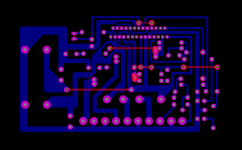
Hello guys,
I've been wanting to build an amp using the lm4780 chip for a while now and I finally have some free time so I searched for a good pcb layout and found this:
in my opinion I think it looks solid but I'm not an expert so I'd like to hear your opinions on it and if the grounding is ok
I've also seen the one in the datasheet but its a double sided pcb and its harder to make so what do you think I should use the one above or the one from the datasheet?
Thanks.
I've been wanting to build an amp using the lm4780 chip for a while now and I finally have some free time so I searched for a good pcb layout and found this:
An externally hosted image should be here but it was not working when we last tested it.
in my opinion I think it looks solid but I'm not an expert so I'd like to hear your opinions on it and if the grounding is ok
I've also seen the one in the datasheet but its a double sided pcb and its harder to make so what do you think I should use the one above or the one from the datasheet?
Thanks.
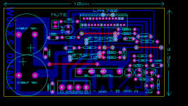
Too small to see - can you make it bigger?
hear you go:
Attachments
Last edited:
Much better thanks!
A number of issues - first its not totally clear which GND point the trafo's CT is going to. Assuming its the one directly below the bridge, there's a problem with the speaker grounds. They share some copper with the main cap charging pulses. They need their own dedicated returns to the CT.
Second - the GNDs (very dirty ones) going to the main caps should not be reused for the mute cap. That really should come from signal GND.
Third - the track from the bridge's -ve output is a wicked noise source and should be kept right away from the output inductors. Suggest a wire on the top side to deal with this.
Much better thanks!
A number of issues - first its not totally clear which GND point the trafo's CT is going to. Assuming its the one directly below the bridge, there's a problem with the speaker grounds. They share some copper with the main cap charging pulses. They need their own dedicated returns to the CT.
Second - the GNDs (very dirty ones) going to the main caps should not be reused for the mute cap. That really should come from signal GND.
Third - the track from the bridge's -ve output is a wicked noise source and should be kept right away from the output inductors. Suggest a wire on the top side to deal with this.
Thanks alot for your advice,
I didn't think there would as many mistakes I'm probably not going to use it now
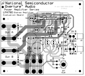
also do you think the one in the datasheet is a good one?
...do you think the one in the datasheet is a good one?
It looks (assuming you mean fig40 in the DS) a little better than the one you posted. It pays lip-service to star grounding which is an improvement. However it does still suffer from my first point - the speaker returns share high current paths with the caps. A definite no-no. Inductors don't look to be fitted so they couldn't make that mistake...

I am working on a similar project with the LM4780 (using the optional external components in figure 6 LM4780 or figure 3 LM3886 data sheet). Active speakers are my intended application. Since it is related, it seems appropriate to post here rather than begin another thread. In the posted picture of your pcb, it appears the heatsink will not have room to sit above and below the board (i.e. chip centered).
Also, not sure if you have already considered the following questions but if you or anyone else can provide feedback, recommendations, or experiences, it would be appreciated.
Q1). When using L//R (for the Thiele network), is there a recommended distance to keep the air core inductor from the LM4780? Or is off the board (but not in contact with the chassis) the best bet?
Q2.) Given the range of experiences reported here when using the Cc, Rf, and Cf parts, is there much harm in leaving the through-hole footprints unpopulated (since these become vias if unused)?
Q3.) Is the LM4780 worth using in the PA100 configuration (described in the National semiconductor data sheets LM4780.pdf and AN-1192) without the DC servo?
Q4.) After reviewing Self's amplifier book, figure 4 of AN-1850, and figure 40 of the LM4780 datasheet, it is unclear where to have the speaker returns. Is it better to have the speaker returns off the board to a separate star ground that consists of the LM4780 pcb GND connection and the output of the DC power board (i.e. after the reservoir caps) gnd connection?
Q5.) While the gnd connection of the LM4780 (pins 12 and 19) are connected to the star end in figure 40 of the LM4780 pdf, would it be better to make the gnd connection to CS7 or off the board to a separate star gnd (as described in the following links)?
LM4780 Dual 60W Audio Power Amplifier
email correspondence with the design support group, here:
LM4780 Audio Power Amplifier - Glenn's Design Log
Q6.) Is there a recommended paper discussing "small loop areas" in PCB designs?
Figure 40 from the LM4780 data sheet is attached below for convenience.
Attachments
Last edited:
A1.)
the inductor should be away from the amplifier and away from any ferrous panels. A couple of inches (50mm) is twenty five times better than 10mm.
A4.)
for a mono block and for a stereo where the two channels are on the same PCB, the Main Audio Ground (MAG) can be on board or off board.
For a stereo where there are two amp PCBs, the MAG must be off board.
Loop area is the area between the signal and its return path.
Estimating Emissions From Your Printed Circuit Board >> Evaluation Engineering
http://www.pcbcarolina.com/images/01_pcb_power_decoupling_myths_debunked.pdf
Estimating Emissions From Your Printed Circuit Board >> Evaluation Engineering
http://www.pcbcarolina.com/images/01_pcb_power_decoupling_myths_debunked.pdf
Hell AndrewT,
Thank you for the reply. Also, your Thiele Networks spreadsheet is helpful as well.
Lastly, are you available via the messaging utility?
Thank you for the reply. Also, your Thiele Networks spreadsheet is helpful as well.
Based on you response in A4.), is it a correct conclusion that the National semiconductor layout (figure 40 shown in my previous post) addresses ground appropriately provided the reservoir ground from an off board power supply is connected to the PCB ground point and that the board is used as a single stereo implementation?A4.)
for a mono block and for a stereo where the two channels are on the same PCB, the Main Audio Ground (MAG) can be on board or off board.
For a stereo where there are two amp PCBs, the MAG must be off board.
Lastly, are you available via the messaging utility?
The way I understand the Output Zobel, then Nat have them in the wrong place...........................Based on you response in A4.), is it a correct conclusion that the National semiconductor layout (figure 40 shown in my previous post) addresses ground appropriately provided the reservoir ground from an off board power supply is connected to the PCB ground point and that the board is used as a single stereo implementation?...................
The star is the MAG in my view. It feeds all the Returns for both channels, except the Speaker Returns.
I can't understand Nat's logic in doing it that way.
Can anyone come up with an explanation that shows the Nat way as being better?
I would ask National.
All the various 'star' grounding schemes are open to discussion and interpretation, there are numerous papers and books that cover the subject, luckily most seem to work, though extensive testing and results especially where rf pick up is involved are far an few in the public domain, and outside most DIYers abilities to test (how many have EMC testing abilities).
The board is an evaluation board, the zoebel's are placed where they are so that there are some to protect the device, when the board is played with, as usually an engineers will just throw some speakers on, better there than none at all.
The way I understand the Output Zobel, then Nat have them in the wrong place.
Can you explain the above statement regarding output Zobel position further? Can you provide a reference for placement location of the output Zobel?
Also, thank you for the output inductor location recommendation. An additional reference pertaining to the output inductor position is presented with position examples and measurements in chapter 8 of Self's Audio Power Amplifier Design Handbook.
The Output Zobel presents an HF and VHF load to the amplifier if the speaker is disconnected or the impedance between the amplifier and the speaker mimics a very high VHF impedance.
To allow the Output Zobel to achieve that VHF loading it MUST have very low impedance, in this case very low inductance.
That can ONLY be achieved by using very short connections from the Output line through the Zobel back to the Power Ground between the decoupling.
These should be just a few millimetres each since the TOTAL Loop Length and Loop Area determines the inductance.
It's a case of reading the relevant literature and understanding what each author is telling us.
A pattern becomes recognisable, even though each Author has their own way of explaining their version.
It's bringing together these disparate thoughts & results that becomes "our personal" understanding.
I cannot recall a single text that states all the points that I am making. Individually each point is usually acceptable and no one objects. It's pulling them all together that gives the useful understanding for me. That's a very personal thing for me. It may not work for others.
An instance where my "understanding" has gone wrong is filtering.
I have described my way of interpreting the information. Knowledgeable Members have come forward and shown I am wrong.
I still cannot see why My interpretation is wrong. But I am working on it.
- Status
- This old topic is closed. If you want to reopen this topic, contact a moderator using the "Report Post" button.
- Home
- Amplifiers
- Chip Amps
- LM4780 PCB Layout