Of all my many designs the only one that hummed was a LM3886 pcb. All the rest were dead silent.
That may be. But you get worse distortion that way. You get the lowest THD you connect the signal ground at the negative speaker terminal. Connect the smoothing caps together and take the centre point of that connection to the PCB. That gets you zero hum and low THD. You can see the resulting performance in the Specifications and Performance Graphs tabs here: LM3886 Done Right: Best DIY implementation of the LM3886 80W gainclone – Neurochrome
I conducted quite a few experiments with grounding in LM3886 amps. You can see them documented here: LM3886 PCB vs Point-to-Point (with data)
And, of course, there're the simulation results I linked to earlier.
Tom
Last edited:
A word to tiefbassuebertr.
I can not say I like the generalized way you seem to condemn every pcb thats out there!
How much do you know about the construction of the chips these amps do come in and how much about in what way does this condition and limit the possible design of a pcb ?
Inside of such a chip-amp there is a die which needs to be connected to the outside world , something which is done by bonding wires which cannot cross over each other , see attached foto of one of these chips.

Therefore the internal construction of the chip and the places inside it where these bonding wires have to be attached conditions which pin of the chip ends up being input , output , positive and negative supply and so on , a sequence which is conditioned by the die itself and cannot be changed freely.
It would be nice and beautiful if pin 1 was poitive input , pin 2 negative input , 13 positive supply , 14 output and 15 negative supply , etc. etc.
As result the sequence of the connections inside the chip conditions the sequence outside it and to a large extend the layout of the pcb in close proximity to the chips pins. ( and not so close )
So you may as well criticize the designers of the die and chip don´t you think?
Another point I think I want to make is that you get what you pay for. Without saying any names ( It is not up to me to advertise and especially not in this forum ) within this very thread there are several good pcb´s mentioned ) obviously you will not get them for 2,95 on ebay. There are a number of other threads where there are very good pcb´s as well both for LM3886 and TDA7294/TDA7293 , and to a lesser extend others as well.
But , if as you say at the very beginning , there is only bad ones around which you do not like you can always go discreete.........which I would do anyways for subwoofers for a number of reasons
Sorry . I dislike generalizations. Michael
I can not say I like the generalized way you seem to condemn every pcb thats out there!
How much do you know about the construction of the chips these amps do come in and how much about in what way does this condition and limit the possible design of a pcb ?
Inside of such a chip-amp there is a die which needs to be connected to the outside world , something which is done by bonding wires which cannot cross over each other , see attached foto of one of these chips.
Therefore the internal construction of the chip and the places inside it where these bonding wires have to be attached conditions which pin of the chip ends up being input , output , positive and negative supply and so on , a sequence which is conditioned by the die itself and cannot be changed freely.
It would be nice and beautiful if pin 1 was poitive input , pin 2 negative input , 13 positive supply , 14 output and 15 negative supply , etc. etc.
As result the sequence of the connections inside the chip conditions the sequence outside it and to a large extend the layout of the pcb in close proximity to the chips pins. ( and not so close )
So you may as well criticize the designers of the die and chip don´t you think?
Another point I think I want to make is that you get what you pay for. Without saying any names ( It is not up to me to advertise and especially not in this forum ) within this very thread there are several good pcb´s mentioned ) obviously you will not get them for 2,95 on ebay. There are a number of other threads where there are very good pcb´s as well both for LM3886 and TDA7294/TDA7293 , and to a lesser extend others as well.
But , if as you say at the very beginning , there is only bad ones around which you do not like you can always go discreete.........which I would do anyways for subwoofers for a number of reasons
Sorry . I dislike generalizations. Michael
Last edited:
I would like to add one note about the pinout of ICs: Most of the time the bond pad locations of the IC are determined from the desired pinout and the design of the lead frame (the metal connections within the IC package that connect from the bond wires to the outside world). If you have control over the IC pinout, you can design it such that it provides the best performance.
In other cases, such as the standard pinout for a single opamp, the pinout is fixed and the bond pads on the IC must be placed to accommodate the pinout. That's why single opamps still have their output on the opposite side of the package from the inverting input even though the two will connect through a resistor or capacitor 99.999% of the time. The pinout for a dual opamp makes more sense, though it would be nice if the power pins were at the same end of the package as that would allow for better decoupling.
I would argue that National Semiconductor did pretty well on the LM3886 pinout. The high-current pins (VCC, OUT, VEE) are in one end of the IC and the sensitive pins (inputs) are at the other. Some "control pins" are in between. That makes pretty good sense to me and makes a good PCB layout fairly straight-forward.
Tom

Currently I have get a Linn LK140 with 2x TDA7294V or TDA7293V for
1) adding CRC snubber network across the secondary winding of main transformer so as
2) the replace of the genuine rectifier by an ultra fast version.
for realizing the first step there are a good descriptions in the links from post 8 under
https://www.diyaudio.com/community/...-3-0s-and-threshold-4000.379674/#post-6921907and under
https://www.diyaudio.com/community/...rmer-snubber-using-quasimodo-test-jig.243100/
For realizing the second step there is a thread under this file (Chip Amps) with various measurements concerning different rectifier diodes performed by the member EVA (from Spain).
Unfortunately I don't find this thread and the associated jpg files.
Maybe one of the member can post this URL - thank you very much.
Here is an extremely helpful website for the LM3886:
https://www.circuitbasics.com/design-hi-fi-audio-amplifier-lm3886/#Balancing-the-Input-Bias-Current
It explains every part of designing an audio amplifier based on the LM3886 in detail.
Hope this helps!
https://www.circuitbasics.com/design-hi-fi-audio-amplifier-lm3886/#Balancing-the-Input-Bias-Current
It explains every part of designing an audio amplifier based on the LM3886 in detail.
Hope this helps!
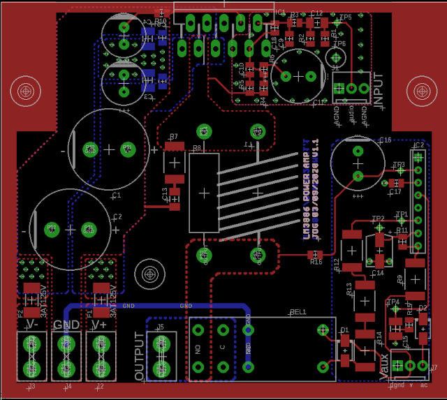
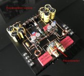
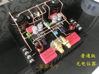
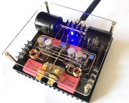
Had some fun doing my own layout. Schematics is roughly the one on the circuitbasics.com site. But I added a protection based on a UPC1237. I used SMD as I have those around. This is the second layout. The first didn't had the fuses in the psu lines and had some issues around the mounting holes where the tracks came too close to the mounting L-brackets. Can't complain about the first version. But I now have to make 8 of them for my active speakers. So I did an iteration. Coil is mounted on the underside. All connection GND go to the power supply pcb, so do the speaker negative terminals.
second image in post #13 under
https://www.diyaudio.com/community/...ication-to-current-drive.389985/#post-7116498
show from my view the best solution for realizing a diy chip amplifier without PCB.
https://www.diyaudio.com/community/...ication-to-current-drive.389985/#post-7116498
show from my view the best solution for realizing a diy chip amplifier without PCB.
In the meantime aliexpress offers amps resp. amp modules in this kind:Are there commercial amps in this kind on the marked (check also the link in post #67) ?
https://id.aliexpress.com/i/1005002277940525.html
https://id.aliexpress.com/item/1005001732955933.html
But the term "Scaffolding Power Amplifier" isn't the right English term - so I think.
What is the right term for this kind of build and solder without PCB in colloquial English ("Scaffolding" means actually a temporary structure on the outside of a building, made usually of wooden planks and metal poles, used by workers while building, repairing, or cleaning the building) ?
Thank you for an advice.
Attachments
-
 LM3886-scaffolding-power-amplifier-TDA7293-scaffoldingoduct-without-transformer.jpg_Q90.jpg_.jpg204.5 KB · Views: 119
 -
 S0b7108b5db7b44ecb58698b88644a5feo.jpg_640x640Q90.jpg_.jpg96 KB · Views: 131
 -
 H53c3bc10464f4ea49539215ae55ed048n.jpg153 KB · Views: 106
 -
 LM1875-scaffolding-power-amplifier-TDA2050-HIFI-power-amplifier-fever-hand-made-power-amplifie...jpg992.2 KB · Views: 113
 -
 LM3886-scaffolding-power-amplifier-TDA7293-finished-product-without-transformer.jpg723.7 KB · Views: 106
 -
 LM3886-Scaffolding-Power-Amplifier-TDA7293-Scaffolding-Power-Amplifier-dengan-Suara-Yang-Indah...jpg96.9 KB · Views: 123
thank you for this URL - a lot of hints there are helpful in general and not only for IC resp. chip amplifiers - e.g. theHere is an extremely helpful website for the LM3886:
https://www.circuitbasics.com/design-hi-fi-audio-amplifier-lm3886/#Balancing-the-Input-Bias-Current
It explains every part of designing an audio amplifier based on the LM3886 in detail.
Hope this helps!
THE GROUND LOOP PROTECTION CIRCUIT (scroll down a bit).
Had some fun doing my own layout. Schematics is roughly the one on the circuitbasics.com site. But I added a protection based on a UPC1237. I used SMD as I have those around. This is the second layout. The first didn't had the fuses in the psu lines and had some issues around the mounting holes where the tracks came too close to the mounting L-brackets. Can't complain about the first version. But I now have to make 8 of them for my active speakers. So I did an iteration. Coil is mounted on the underside.
From my view this is the best way as long as this is those GND solder joint of both capacitors behind the rectifier.All connection GND go to the power supply pcb, so do the speaker negative terminals.
But as one know, there are different views as to which variant of GND management is the best in terms of playback quality e. g. the question, whether one run the GND connection of the input filter (RC) at the non-inverting input and the GND connection of the NFB resistor (from inverted input) via separate wires or via a single wire for both to the GND of both caps bhind the rectifier.
Exact investigations regarding different GND managements and it's consequences were described in a very interesting article in German's electronic magazine "FUNKSCHAU" (approximately 35-40 years ago) - for the chip amp - I think, with TDA2030 or TDA2040.
Unfortunately I don't find this issue (26 issues/Year).
Maybe one of the member know this - thank you very much for an advice.
- Home
- Amplifiers
- Chip Amps
- Why are there only disastrous PCB Versions for TDA7293/TDA7294/LM3886 etc. available?