Leave them in. They don't contain L to form resonant circuits. Those caps are snubbers for the rectifier's switching noise.
The L would be in the large electrolytics and/or the PCB traces. The 100 nF would most likely be a very low loss film cap.
This subject (paralleling small film caps with electrolytics) has been discussed at great length and it has been shown that
a) they cannot do anything that is useful unless they are very near the load, and,
b) they create a risk of a high-frequency resonance.
If you want film caps, there, then use some that are at least 10% of the capacitance of the electrolytics, or at the very least some that have enough capacitance (at least 10s of uF) that they can work through the relatively large parasitic inductance of the lengths of the power/ground rails between the film cap and the load.
If you "feel" that you must have small film caps, there, then place a low-value resistance in series with each of them, to damp the resonances.
If the intended purpose of the 100nF caps is to suppress spikes from the rectifier diodes, then a snubber should be used, instead.
A capacitance is not a snubber. A resistance is a snubber and it should be the correct (optimal) resistance, i.e. the characteristic impedance of the LC circuit as seen at that point.
To determine the optimal snubber resistance for an existing circuit, see
http://www.diyaudio.com/forums/powe...lm-caps-electrolytic-caps-30.html#post2828689
for a simple practical method.
As noted, the only reason for a capacitor in a snubber or terminator network is to limit the dissipation in the resistor by passing only unwanted frequencies to it, if the needed resistance value is too low.
In rare cases, one might be able to find a capacitor that has an ESR (equivalent series resistance) that is the needed value for the snubber resistance for a particular circuit.
But blindly throwing in a 100 nF cap, without determining the optimal damping resistance and matching the cap's ESR to the needed snubber resistance value at the frequencies of interest, and then also determining the needed capacitance value, is often worse than doing nothing.
Last edited:
Are you are selling PCBs using information given out for free on this Forum?
Hi Andrew
The answer to the question is yes.
He is selling a LM3886 PCB for $2 to $3. Really. I have not bought any of them because I already had mine on order before I knew about these ones, which are cheaper to access than any kind of product from anywhere.
Whereas at a level of principles it is a semi-commercial venture, it is definitely a very attractive service (at least to the DIY community in India, which is treated like a pariah by our local industry). Given that you can take a call whether you should continue to contribute to this thread (I wish you would).
@Kuldeep, This PCB seems to be really large. I do know you have the power supply on board, but consider a perforation in the board with jumper links (Peter does this beautifully on his LM4780 boards) so that the PS can be removed, and also along the length to result in mono boards. The reason is that this has possibilities for DIYers to integrate these into compact PC theater solutions in multichannel configurations. The way you have designed it makes it suitable only for stereo applications, a little flexibility might help.
In any case your design indicates that solid wires will be needed to wire the supply to the amplifiers. I don't see the point of putting components on a board then using wires to hook them up.
On the board itself, it again seems overly complex. You may want to go down one size resistor (1/8W works great). My 1875 P2P builds usually never exceed the footprint of the chip. I do know you cant achieve that with a PCB - but maybe you can.
On your squiggle - I would suggest putting the resistor pads back, that way one has full control over whether they want it or not. A PCB trace modification is not as easy as choosing between a resistor and a jumper. Needless to say the resistor isolation comes with its own issues.
Connectors are much easier to access, connect and solder to free wires when they are at board edges. They also free up space within the board and make clean wire management a possibility. See if that helps you, I'm particularly thinking about the power and input connections. I would see that freeing up a lot your problems with the layout - but at the level of a single board.
The routing looks very untidy - on this I agree with everyone. Try drawing it first on a piece of paper. It will need to be rethought. Just moving stuff around will not work. I might suggest using more resistors vertically. The chip is divided into two 'halves', with the left handling the low-level signals and the right handling high currents. Visualise the flow of current and it'll be easier to crack a good layout. I would suggest staying away from planes for your first designs, and instead using two paths per chip, one for each kind of current and returning only those connections that are absolutely essential.
One reason I use few PCBs is that most are terribly designed, I only resort to buying PCBs for non-critical applications such as home theater. It's much easier to route currents when you do it by hand.
Good Luck.
very well. now this thread is going on all together different direction. First of all let me clear this is not a business for me. I am very well settled in a well paying defense job. And sangaram, Yes, i have been selling only LM3886 PCB (single sided) for just 2$. What do you expect lesser than that. And you will not believe 3 years back i have made hand fabricated and drilled PCB for LM4780 & 3886 only for pure hobby purpose and some surplus PCBs i also "sold" to some indian Diyers for. I had given full information how to make your own PCB with drilling at home posted on blog from last 4 years. And none of the information is copied from this forum anywhere.
Now i am proud to say with my own experimentation and matured knowledge of LM3886 & 4780 layout i have made a commercial PCB fro 3886 alone, which costed me 80 Rs/- per piece (which i am offering to sell @100/-). And today i got a quotation of Rs/- 1500 for 5 PCBs of dual layer LM3886. I will be ordering that knowing that this is only my risk and interest. What do u expect, will anyone in India buy that LM3886 PCB for Rs. 300/-. But i want to make availability of such PCBs in India.
With the same interest only i proposed to make this stereo amplifier board, and now i am feeling i did a mistake of posting on this forum. The PCB for amplifier alone is very much fine tuned. I only wanted to fine tune the power routing. People are accusing me of making profit from this forum which i feel is ridiculous. If you see my profile i have previously posted many amplifier PCBs which were made by me only. My intention had always been sharing of know how only.
I have not bought any of them because I already had mine on order before I knew about these ones, which are cheaper to access than any kind of product from anywhere.
What you want to say, are you also selling PCBs.
In any case your design indicates that solid wires will be needed to wire the supply to the amplifiers. I don't see the point of putting components on a board then using wires to hook them up.
This is a single layer design. So with out wires i cannot connect them.
On the board itself, it again seems overly complex. You may want to go down one size resistor (1/8W works great). My 1875 P2P builds usually never exceed the footprint of the chip. I do know you cant achieve that with a PCB - but maybe you can.
This board looks complex to you, its an easiest layout of which one can think of. I am using common available components, 1/4 w is most available. I have also made 1/8W for an another project, but i know how difficult was to source them.
I didn't get what you are trying to convey. Is it about Signal_ground resistor.On your squiggle - I would suggest putting the resistor pads back, that way one has full control over whether they want it or not. A PCB trace modification is not as easy as choosing between a resistor and a jumper. Needless to say the resistor isolation comes with its own issues.
The routing looks very untidy - on this I agree with everyone. Try drawing it first on a piece of paper. It will need to be rethought. Just moving stuff around will not work. I might suggest using more resistors vertically. The chip is divided into two 'halves', with the left handling the low-level signals and the right handling high currents. Visualise the flow of current and it'll be easier to crack a good layout. I would suggest staying away from planes for your first designs, and instead using two paths per chip, one for each kind of current and returning only those connections that are absolutely essential.
All the other people didn't say it tidy or untidy, is the functionality that's important. And i will not use vertical resistors, every vertical resistor adds extra length of wire. And my design is same way as you have mentioned. Input on left side, output on right side and power supply in center.
The trickier job is to place 2 ICs side-by-side where output of left IC is closer to input of right. And i have kept maximum possible separation between them. And i feel its very much OK, considering the distances of wires & signal inside the Chip die itself.
You have completely misunderstood me. Please read my post again with deep breaths, and you'll see that I was appreciating your efforts. I see that you have taken offense and I shall desist from contributing on the thread.
As long as you're happy with the board, good for you. All the best with your project.
As long as you're happy with the board, good for you. All the best with your project.
..is not the subject. They are snubbers for the rectifier's switching noise.This subject (paralleling small film caps with electrolytics)
They should be ceramic caps.If you want film caps
A snubber is anything that snubs up something.A capacitance is not a snubber.
Capacitors are great snubbers for HF, like e.g. switching noises, because they have extremely low impedance there. HF is snubbed by simply shorting it. A series resistor would reduce the effectiveness by increasing the resistance in the path. The only reason to add a resistor is to tune the snubber's resonant frequency to the switching noise's frequency. To do that you need to determine the latter, which is usually not practical in a DIY environment.
A single resistor without capacitor will not be as effective at HF, but will create losses at LF.
The absolute capacitor value is not important. Values in the tens to low hundreds of nF are good-practice compromises between the contradictory goals of small cap for high snubbing efficiency at HF and big cap for lowest possible frequency where noise can effectively be suppressed. 100 nF is quite OK.
Thanks folks,
The tips i got are, i need to redesign the power supply layout by
1. the 100nF near the rectifier can be omitted and the 100nF near the ICs may be sufficient for HF suppression.
2. I need to divide the ground plane going to +ive power caps and the right channel output ground.
3. And the zigzag trace to be avoided, may be i provide a ground resistor of 2R2.
4. Provision to include different sizes of input caps & non-polarized zobal cap.
& May be a thicker "Audio output trace for Both ICs.
I'll update the PCB shortly.
..is not the subject. They are snubbers for the rectifier's switching noise.
They should be ceramic caps.
A snubber is anything that snubs up something.
Capacitors are great snubbers for HF, like e.g. switching noises, because they have extremely low impedance there. HF is snubbed by simply shorting it. A series resistor would reduce the effectiveness by increasing the resistance in the path. The only reason to add a resistor is to tune the snubber's resonant frequency to the switching noise's frequency. To do that you need to determine the latter, which is usually not practical in a DIY environment.
A single resistor without capacitor will not be as effective at HF, but will create losses at LF.
The absolute capacitor value is not important. Values in the tens to low hundreds of nF are good-practice compromises between the contradictory goals of small cap for high snubbing efficiency at HF and big cap for lowest possible frequency where noise can effectively be suppressed. 100 nF is quite OK.
Sorry. No. That's mostly incorrect. Snubbing is not like bypassing.
Snubbers work by damping a resonance, which requires, and only works because of, a resistance.
The optional series capacitance is used only if it's needed, only to limit the power dissipated in the snubbing resistance by blocking frequencies other than those needing to be damped.
The series resistance is the only thing needed to make a snubber damp a resonance effectively (if power dissipation were not a concern).
The snubber resistance is tuned to be equal to the characteristic impedance of whatever LC resonance it is placed in parallel with, i.e. √(L/C), where L and C are often parasitic inductance and capacitance.
That resistance value gives maximum damping of the resonance, which optimally minimizes the amplitude of the overshoot, ringing, reflections, etc (depending on the type of circuit) that were caused (or allowed) by the LC resonance.
The series capacitance value, if needed, actually is important, since it should allow the snubbing resistance to be seen by the unwanted frequencies but not allow it to be seen by the desired working frequencies of the circuit, in cases where it would then dissipate too much power.
If the series capacitance is needed, its value should be about 4X the parasitic capacitance, C (from above), but could optionally be up to 10X C, which would give a slight further reduction in voltage overshoot amplitude (compared to 4X C) at the expense of higher dissipation in the snubber resistance.
Finding the optimal snubber resistance value is not difficult and almost any DIYer should be able to do it quickly and easily, if they have the use of an oscilloscope that can measure the frequency of the overshoot/ringing voltage that needs to be snubbed.
The simple short procedure is posted at the link I gave. But below are the steps. (Note that even though the L and C are referred-to as "parasitic", they can also include effects from actual inductors and capacitors.)
PRACTICAL SNUBBER AND TERMINATION DESIGN:
This procedure assumes that there is a ringing or overshoot condition, already, such as might occur on a digital buss or a transmission line or PCB trace, or in a switch-mode power supply or even an AC-to-DC transformer/rectifier circuit, and in many other types of circuits.
1. Measure the frequency of the resonance or ringing, using an oscilloscope (or a circuit simulator, if you've modeled the parasitics well). Use f = 1/period, where period = time for one complete cycle, or, if a whole cycle is not visible, either measure time for 1/2 cycle, or, use f = 1/(π trise) where trise is the rise time.
2. Add a shunt capacitor and adjust the value of this capacitor until the frequency of the ringing is reduced by a factor of two. I've left out the math but the value of this resulting capacitor will be three times (3X) the value of the parasitic capacitance that is creating the resonance.
3. Because the parasitic capacitance is now known, the parasitic inductance can be determined using the formula:
L = 1 / [(2 · Pi · F)² · C]
where F = (original) resonant frequency and C = parasitic capacitance determined above.
4. Now that both the parasitic capacitance and inductance are known, the
characteristic impedance of the resonant circuit can be determined using the following formula:
Z = √(L/C)
where L = parasitic inductance and C = parasitic capacitance.
5. The resistor value used for the terminator or for the RC snubber circuit should be equal to Z, the value of the characteristic impedance, and the capacitor, if needed, should be sized between four and ten times the parasitic capacitance. The use of larger (than 4X) capacitors slightly reduces the voltage overshoot at the expense of greater power dissipation in the resistor.
NOTE: The resistor, alone, is all that is needed to prevent or damp-out the ringing (or reflections, as the case may be). But if power dissipation in the R would then be too high, a C is added in series with the R, so that only the unwanted frequencies cause currents in the resistor. (And that, boys and girls, is the only reason there's a capacitor in a snubber.)
Last edited:
I propose to have a look at commercial amp schematics. Small caps across the rectifiers are quite common, resistors very rare. An interesting read in that context may be National's AN-1849. Those capacitors are mentioned on the first two pages.The optional series capacitance is used only if it's needed, only to limit the power dissipated in the snubbing resistance by blocking frequencies other than those needing to be damped.
Experience has it that only relatively few DIYers have access to an oscilloscope.almost any DIYer should be able to do it quickly and easily, if they have the use of an oscilloscope
I propose to have a look at commercial amp schematics. Small caps across the rectifiers are quite common, resistors very rare. An interesting read in that context may be National's AN-1849. Those capacitors are mentioned on the first two pages.
Experience has it that only relatively few DIYers have access to an oscilloscope.
I do see the 0.1uF (100nF) caps across the diodes in the PSU schematic in AN-1849, which they say are filters, not snubbers.
Here is what it says on Page 2, about those capacitors across the rectifier diodes:
"CS11 - CS14 are in parallel with the bridge diodes to reduce
high frequency noise and ringing of the diode. An
additional RC snubber in parallel with each diode of the
rectifier will further reduce noise and ringing."
Whenever I see 0.1uF caps, I often wonder if the designer was one of a) just lazy or b) they just didn't understand enough about what they could and should be doing, or c) understandably time/cost-constrained. The probability of the best C value being 0.1uF in so many places in so many designs is rather low, to put it mildly. So they're almost always just the result of people applying a "rule of thumb". Sometimes it's OK and other times it's not. But you can be pretty sure that no analysis or calculations were done, when you see one. (Sometimes it matters not at all. Other times, a DIYer should take advantage of having the luxury of being able to try to do it the best way.)
And sure enough, here is another quote from Page 2 of AN-1849:
"The values for the different capacitors were not chosen based
on extensive bench work or research. The values were chosen
based on general guidelines and commonly used values.
Additional performance may be obtained through refinement
of the capacitor values. The equations and methods to determine
optimal values are beyond the scope of this application
note."
Anyway, there are four or five good papers available on the web, if you google for "snubber design". You could probably also add "rectifier" to that and find some good stuff, too.
-----
Almost every serious circuit-DIYer I know has at least one oscilloscope, or access to use one. I built a heathkit scope when I was 11 years old (still have it). The kit cost about $24 new, I think. But that was a lot of money back then (1968 or so). Ebay is usually full of cheap scopes, here, nowadays. I also got a few good Tektronix scopes from military DRMO sales, like 453, 475, 2235, 2465, 7603, 7904A, et al.
Last edited:
I built up a Power Amplifier from a module and schematic precisely detailing the whole electrical section from Mains transformer through to speaker terminals.I propose to have a look at commercial amp schematics. Small caps across the rectifiers are quite common, resistors very rare. An interesting read in that context may be National's AN-1849. Those capacitors are mentioned on the first two pages.
It blew up. Working with the designer, it was rebuilt and it blew up again.
Still working with the designer, it was rebuilt again. This time I went back and had another look at the PSU. There were the specified 100nF caps across each diode of the bridge rectifier. They were directly the cause of the instability of the amplifier. They changed the frequency of the ringing on the PSU, but did not damp the ringing out. Removing them completely removed the tiny ripple that was only just visible. That was enough to get the amp to last a lot longer before blowing up again. I gave up.
Most of the time c), sometimes a), every now and then b)I often wonder if the designer was one of a) just lazy or b) they just didn't understand enough about what they could and should be doing, or c) understandably time/cost-constrained.
You find values from the tens to the low hundreds of nF, not only 0,1 µF. Most designers test and measure before they let a design loose on the world. Their mission is not always to build the best solution, but to meet certain specs. 0,1 µf is probably the Pareto solution that gives you 80% of the best possible result with 20% of the effort which is sufficient for most designs. I'd rather take the 80% solution than nothing, if I had no oscilloscope.The probability of the best C value being 0.1uF in so many places in so many designs is rather low, to put it mildly.
That can be one of the purposes of DIY, to get a better device for the same money by putting in more effort than a type c) designer is allowed to.a DIYer should take advantage of having the luxury of being able to try to do it the best way.)
A great number of the people in the Chip Amp section appear to have different goals, though. Cheap, small and simple are the prevailing preferences.
Probably in different sections of the Forum. Here in the Chip Amp section you come across people that try to build amps without even a DMM.Almost every serious circuit-DIYer I know has at least one oscilloscope, or access to use one.
So the different ringing frequency pronounced the amp's imminent issues. But would it have improved the performance of another amp without built-in stability problems?Removing them completely removed the tiny ripple that was only just visible. That was enough to get the amp to last a lot longer before blowing up again. I gave up.
I built up a Power Amplifier from a module and schematic precisely detailing the whole electrical section from Mains transformer through to speaker terminals.
It blew up. Working with the designer, it was rebuilt and it blew up again.
Still working with the designer, it was rebuilt again. This time I went back and had another look at the PSU. There were the specified 100nF caps across each diode of the bridge rectifier. They were directly the cause of the instability of the amplifier. They changed the frequency of the ringing on the PSU, but did not damp the ringing out. Removing them completely removed the tiny ripple that was only just visible. That was enough to get the amp to last a lot longer before blowing up again. I gave up.
Maybe you should have tried snubbers.
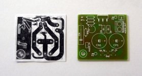
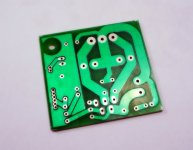
Made my final design.
After many iterations, i finally opted to go for single chip version. The idea of putting stereo chips and power supply was giving me headaches on fine tuning. Here is the final layout and i also got some PCBs fabricated. Will populate a stereo pair of amplifier shortly")
After many iterations, i finally opted to go for single chip version. The idea of putting stereo chips and power supply was giving me headaches on fine tuning. Here is the final layout and i also got some PCBs fabricated. Will populate a stereo pair of amplifier shortly
Attachments
- Status
- This old topic is closed. If you want to reopen this topic, contact a moderator using the "Report Post" button.
- Home
- Amplifiers
- Chip Amps
- Stereo LM1875 / TDA2050 PCB with Power Supply