Hi friends,
I am planning to make a Stereo PCB for LM1875 / TDA2050 with Power Supply. Just finished with initial PCB routing. The power supply routing will be converted to planes and there will be a central ground plane.")
I am planning to make a Stereo PCB for LM1875 / TDA2050 with Power Supply. Just finished with initial PCB routing. The power supply routing will be converted to planes and there will be a central ground plane.
Attachments
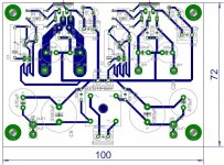
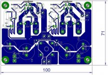
I made planes now as shown. Trying to fine tune the ground plane.
Since its a single side PCB, the +- supply lines needed to be connect by jumper wires, VP_out <-> VP_in and VN_out <-> VN_in.
And the zig zag trace connects signal ground to main ground, its a kind of experiment only, i expect it to simulate 1Ohm ground resister. But i hope it doesn't cause any inductive effect. (Mr Andrew, kindly give your opinion on this). And the "one" you mentioned, i plan to make that at GND terminal connector, which also connects to transformer's center tap.
Attachments
Last edited:
@ pacificblue
Then will widening the zigzag trace will inductance to minimum level at the same time providing a longer trace for signal ground. The only idea is to raise the signal ground from main ground without using any resister. Is it acceptable.
And the transformer canter tap will connect to GND header (just above the bridge rectifier). I am using 0.1uF at output zobal, ya, that can be converted to non-polarized cap.
And Mr. AndrewT, I got your point, but it will be more easy to apply that in double sided design. In my place the PCB fab cost doubles for Double sided PCB, and that's why i have difficulty to terminate all ground traces to a single point in single side PCB.
Last edited:
It's your single sided that is wrong.............but it will be more easy to apply that in double sided design. In my place the PCB fab cost doubles for Double sided PCB, and that's why i have difficulty to terminate all ground traces to a single point in single side PCB.
Don't complicate it with double sided. Learn how to do single sided first.
Widening it won't make a big difference for the inductance. Ground traces should not be meandering.Then will widening the zigzag trace will inductance to minimum level at the same time providing a longer trace for signal ground.
A 0,254 mm wide 35 µm thick trace will approximately have 1 Ohm for every 50 cm of length. There should only be one signal ground for both channels.The only idea is to raise the signal ground from main ground without using any resister. Is it acceptable.
In addition, any component that connects to a chip pin should be connected as close to the pin as possible, with priority given to capacitors that connect to power pins, from smallest to largest. And all path lengths should be kept short.
Your top resistor (in the group of three to the left of the chip) should be placed directly behind and centered against the pads for the two pins it connects, for example, and the other two resistors should be right up next to the pads they connect to. And the two capacitors for each power pin should be much, much closer to those pins.
And you should fill all of the open areas with ground plane, when you're finished arranging everything.
Hello Mr. Gootee, how r u... Sure, we can do that as you told but again it will change the whole PCB layout
What is your point? You don't want to correct your layout?
That's your decision to make, of course. But the suggested changes would be rather trivial and the layout is relatively small and simple and easy to change. And the current layout has significant problems and does need to be changed.
P.S. Another needed change that I just noticed: Your input signal and signal ground paths should stay as close together as possible. Yours currently form some enclosed loop area which will act as an antenna for AC hum as well as RF (See Faraday's Law.). The signal input section is probably the worst place to have that situation. It would be easiest and probably also best if you just filled that whole area with ground plane, all the way up to close to the + input pin (but probably not around the - input pin or its components).
Also, R9 and R10 (of your Zobel networks) need to be connected as close to the output pins as possible. And the capacitors in the Zobel networks are typically film types. And the output trace is another one that should have ground close to it, all the way up near the output pin. You will also twist you putput signal and ground wires together, at least until they are away from the rest of the circuit.
And, the 100 nF caps near the rectifier bridge should probably be removed so there won't be a danger of having them form high-frequency resonant LC circuits with the large electrolytics and/or other parasitic inductances.
And, you should add a 470 pF capacitor from each LM1875's + input pin (Pin 1) to ground, to form low-pass RF filters (with the 1K resistors R1 and R5) with a cutoff frequency of about 300 kHz.
You will also want to fill the area between each pair of large DC traces that connect to the chips with ground plane, to lower the enclosed loop areas of your DC power rails. You will, of course, also be routing their supply wires right against the copper ground plane.
Also remember to tightly twist together the incoming AC mains wires. I would also increase the gap between the AC-carrying copper and everything else, as much as possible.
You also need to force the rectified AC to pass directly through the pins of the smoothing caps and not leave a large area around the pins. For the larger caps, you can just put a narrow slot in that plane, from each cap's "AC" pin to the edge of the board. But you will have to move them, toward the rectifier, so you can make room to also move the 470 uF ones in the same direction, then make a slot from each of the two 470 uF caps' "AC" pins to the edge of the board, and then have the DC power connection points past them, nearest to the right and left edges of the board.
You will not enjoy having such small pad rings on your input capacitors. Also, you should add a trace that goes nost of the way between that cap's pads, with holes for different lead spacings, in case another type of cap is used.
Acute angles (less than 90 degrees) should be changed, or have chamfers added, so that all angles between any copper edges, everywhere, are greater than 90 degrees.
Last edited:
Hello Mr. Gootee and Mr. Andrew. With all due respect i didn't meant to be rude. The problem happened is that my daughter has deleted the whole folder of my eagles files and accidentally run ccleaner also. Now only thing remaining of this "Stereo amp project" are the pictures i posted
But Big thanks to Mr. Gootee, he mentioned some gr8 points regarding power supply design and other points on layout. Now i am thinking maybe putting 2 chips and power-supply on single PCB may not be a good idea.
My constraint is that in my previous design of LM3886 PCB, i had not included the power supply design and some 8 people who brought my PCB, all had different power supply arrangement, and all gave different types of feedback regarding sound output.
And if i make a separate PCB for Power supply, it adds to costs are not many people are willing to buy it. So i thought this time to design this Stereo amp kit with power supply.
I think now I can re-design the layout starting from scratch and keeping these new points in consideration.
Are you are selling PCBs using information given out for free on this Forum?
Ha haa.. Yes, i been making 100$ per PCB
Don't worry, i am just joking. You know if its about money, i wouldn't have sticked to this diyaudio forum from last 6 years and running my own blog DIY Audio Amplifier Blog free of cost (& You don't need to register an account to see my blog).
Anyone who wanted to make money would simply copy the gr8 Brian_gt PCB and carlos_fm power supply and even need not to declare that on this forum and silently make a lot of money.
And, the 100 nF caps near the rectifier bridge should probably be removed so there won't be a danger of having them form high-frequency resonant LC circuits with the large electrolytics and/or other parasitic inductances.
Leave them in. They don't contain L to form resonant circuits. Those caps are snubbers for the rectifier's switching noise.
- Status
- This old topic is closed. If you want to reopen this topic, contact a moderator using the "Report Post" button.
- Home
- Amplifiers
- Chip Amps
- Stereo LM1875 / TDA2050 PCB with Power Supply