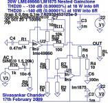
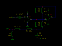
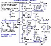
Here's a first attempt to apply an LME49860 op-amp as a front-end along with an LM1875 as the power stage, with a nested-feedback schema. The topology is vaguely reminiscent of Technics/Class S circuits, but has some improvements. The initial simulation results are excellent - the THD20 numbers are much better than the LM1875 alone exhibits.
Edit: Thanks to Pedja for his LM1875 model.
Edit: Thanks to Pedja for his LM1875 model.
Attachments
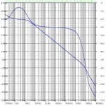
Here's the closed-loop AC small-signal response. With C7 = 10 pF, as shown, the response rolls off rapidly above 1 MHz. Increasing the value of C7 to 22 pF or 47 pF will roll off the response at a lower frequency, with a small cost (a few dB higher) in THD20.
Attachments
R12 = 39k is part of the nested inner feedback loop for the LME49860, which linearizes it substantially. I determined the values of the feedback resistances empirically by simulation, but these are by no means optimal.
There are some stability constraints, however. R7/R2 sets the gain for the LM1875, and that has to be greater than 10. R8/R5 has to be almost exactly equal to R7/R2, to minimize the feed-forward current contribution of the LME49860 through R3 (100 ohms). R3 cannot be too low, or U2 will go into current limiting (U2 contributes a small amount of feed-forward correction current directly to the load through R3).
The Boucherot RC cell has typical values found in similar designs, but it might aid stability if the R is reduced further to 2.2 or 4.7 ohms (this will increase the dissipation in the Boucherot cell, however).
There is some scope to play around with some of the feedback resistor values, and it is likely that these can be optimized further by simulation.
It has also been brought to my attention that my topology is broadly similar to Mauro Penasa's LM318/LM3886 gainclone - and indeed, the main ideas are the same: a front-end op-amp, with nested feedback (around the front end, and globally). There are some uncanny similarities (notably, the substitution of the Zobel inductor by a small resistor in both topologies), but my topology is simpler and includes a key element missing in Penasa's gainclone: feedforward error-correction from the front-end opamp (the LME49860) directly to the load. I have avoided the use of reactive bridging or compensation where possible, and there is only one externally introduced pole - from C7 (10 pF).
Ideally, we'd like to minimize the feed-forward current, but it's not possible to keep the phase of the signal from the LME49860 the same as that of the signal from the LM1875. The main reason is that there are internal poles, including a dominant pole, in the LM1875, which will cause a slight lag in output waveform. Hence, there will be a small difference between the two signals at all frequencies.
One can omit R3 totally (similar to Mauro Penasa's design), of course, but THD will increase without the feed-forward current component. It will still be better than the LM1875 alone, because the front-end LME49860 is still within the feedback loop.
One can omit R3 totally (similar to Mauro Penasa's design), of course, but THD will increase without the feed-forward current component. It will still be better than the LM1875 alone, because the front-end LME49860 is still within the feedback loop.
Hi, Linuxguru,
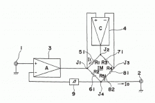
I don't clearly understand how this bridge works in patent #4,716,378. Amplifier A is the main amplifier, provide voltage swing. Amplifier C is current amplifier.
What is the gain working on amplifier C? Is it unity gain? If it needs unity gain stable amp, we cannot use chipamp for amplifier C.
I don't clearly understand how this bridge works in patent #4,716,378. Amplifier A is the main amplifier, provide voltage swing. Amplifier C is current amplifier.
What is the gain working on amplifier C? Is it unity gain? If it needs unity gain stable amp, we cannot use chipamp for amplifier C.
Attachments
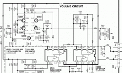
I don't necessarily understand the Technics schematic of the previous posting - it seems to be entirely small-signal, i.e. pre-amp only. I'll look into it later to try to glean insights, but for now I'll skip it.
In the patent diagram in post #9, the closed-loop voltage gain of C can be calculated. There's voltage-series feedback through R3 and R4, R5 and RL (not shown). Assuming ideal op-amps A and C (zero input offset, zero input current, infinite open-loop gain), and a lot of high-school algebra, we get the following expressions for the voltages at nodes J2 and J3:
Vj2 = Vo (1 + (R2 (R3 + R4 +R5) / (RL(R2 + R4 +R5)))) ..... (1)
Vj3 = Vo (1 + (R2 (R4 + R5) / (RL (R2 + R4 + R5)))) ..... (2)
Voltage gain of C is simply Vj2 / Vj3, which simplifies (after more algebra) to:
Vj2 / Vj3 = 1 + R2.R3 / (R2(R4 + R5) + RL(R2 + R4 + R5))
Since all the Rs are positive, we see that the voltage gain of C is necessarily greater than unity. That's a big relief, because that was also intuitively obvious just by inspecting the circuit topology in post #9, and it's nice to see that intuition doesn't conflict with the analysis.
In this particular case, the gain was greater than unity, but there may be other bridge topologies (notably the quad current-dumping topology), where the voltage-gain of the output stage is required to be 1 or very close to 1. This requires the use of unity-gain stable amplifiers, or alternatively, to attenuate the voltage input to the output stage by a factor equal to its minimum stable closed-loop gain, and set its closed-loop gain to the reciprocal of the attenuation factor to recover unity gain.
In the schematic of post #1, the attenuation is 1k/(1k+10k) = 1/11, and voltage gain of the LM1875 has been set to (1 + 10k/1k) = 11. The LM1875 is spec'ed to be stable at gains over 10, so it's stable as shown. For other chipamps with differently specified minimum stable closed-loop gains, we have to adjust these dividers accordingly. For the TDA7294, the minimum stable closed-loop gain is specified to be 24 dB => a gain of ~16 or higher.
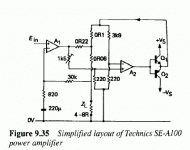
It's RL, load resistance (not shown in the patent diagram). The SE-A100 schematic differs from the patent diagram in some respects - notably, the attenuator to the output stage is grounded in the SE-A100 (as it is in my nested gainclone schematic), but in the patent diagram of post #9, the load forms part of the attenuation network (this has consequences for stability under no-load conditions, etc.)
The schematic in post #13 is also a Technics-like topology, and has some conceptual similarity to my nested gainclone. The main difference is the impedance of the networks, as well as the low-impedance path from the chipamp to the load.
The schematic in post #14 is also a similar Technics-like topology. The main difficulty in realizing these in practice is the consequence of bridge imbalance. Not only could the small-signal front-end opamp go into current limit, its output stage could also be damaged. There's a need to isolate the output of the chipamp from the output of the op-amp, with a resistance of ~ hundred ohms, rather than a fraction of an ohm.
Hi, Linuxguru,
I try to calculate gain for amp C with this formula
Vj2 / Vj3 = 1 + R2.R3 / (R2(R4 + R5) + RL(R2 + R4 + R5))
R2=10ohm, R3=10k, (R4+R5)=1k, RL=600ohm.
With RL=600ohm, the gain is very near 1 (unity gain). I guess this means that amp C should be unity gain stable.
Why is in equation above there is no R1 at all?
> Why is in equation above there is no R1 at all?
Good question, and for a moment I feared that my math was wrong. Then I figured out why the math is right, and R1 doesn't enter the equations: The voltages at all nodes are fully specified by the rest of the circuit, and R1 will not enter the equations to calculate the node voltages.
With ideal op-amps (with infinite current sinking/sourcing capability), both sides of R1 are driven by norators (hypothetical devices that can source any current at any voltage). Hence, any value of R1 is admissible, and the voltages at each end of R1 will still remain the same - only I1 depends on R1.
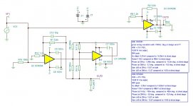
After playing around in LTSpice for while, I came up with another nested gainclone concept similar to Walt Jung's composite op-amp/buffer. I dropped the feedforward path and retained some gain in the power op-amp stage, thus keeping the voltage swing at the output of the small-signal op-amp low. This allows the use of a jelly-bean ne5532 as the small-signal op-amp and still retain good performance.
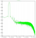
Of course, one could substitute the ne5532 with something better, like an LT1208 or an LT1469 or an LM4562. However, it will been seen from the simulation results that the NE5532 does very well indeed when its swing is kept low - around 1 V peak. How well? The nested gainclone topology reaches ~ -120 dB THD20, mostly H2. In fact, almost all the distortion is even harmonic.
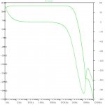
Here's the LTSpice simulation schematic - it uses a loop probe injection method, due to Tian et al (and simplified by Wiedman), to determine the AC small-signal loop gain, phase margin and stability. The sources Vi and Ii in the schematic are used to implement the probe - These do not enter the LTSpice large-signal transient analysis.
Of course, one could substitute the ne5532 with something better, like an LT1208 or an LT1469 or an LM4562. However, it will been seen from the simulation results that the NE5532 does very well indeed when its swing is kept low - around 1 V peak. How well? The nested gainclone topology reaches ~ -120 dB THD20, mostly H2. In fact, almost all the distortion is even harmonic.
Here's the LTSpice simulation schematic - it uses a loop probe injection method, due to Tian et al (and simplified by Wiedman), to determine the AC small-signal loop gain, phase margin and stability. The sources Vi and Ii in the schematic are used to implement the probe - These do not enter the LTSpice large-signal transient analysis.
Attachments
- Status
- This old topic is closed. If you want to reopen this topic, contact a moderator using the "Report Post" button.
- Home
- Amplifiers
- Chip Amps
- LM1875 nested Gainclone