Hi,
@KSTR #33
nice finding with the Diode indeed.
THD starts increasing way before the current clipping point is reached, but as You said ... it somehow gracefully slips into a kind of class-B mode.
Heat power losses need to be watched though, as the Vgs of the JFET becomes positive above the clipping point ... with an increase of current above the Idss value and associated heat development.
While the SEPP of #39 (when modified as in the attached .asc) remains very low in doistortion as long as it stays in the class-A range, but clips sharply with correspondigly jumping up THD figures, when the current cuts off.
@ElFishi
Q4 only reduces the supply line here.
The Buffer´s positive peak output voltage is limited to values below Q4´s emitter voltage.
Increasing R9 to 47k would raise that limit considerably.
Also the parts values and schematic around the CFP part could be modded like in the asc giving better results.
The current distribution between JFET and bipolar can be set easier and precise with the modded circuit.
And using the same CFP for a modulated CCS like in #7 then spares the NPN and both Follower and CCS have similar temperature tracking, so output offset voltage drift remains low and You may omit with a output Cap.
jauu
Calvin
Attachments
I haven't build the CFP version yet, I'm not near a solderng iron atm.
But I did build a Borbely-style source follower/CCS buffer with BF862 and had precisely the problem I described above: 20k Pot at the gate of the BF862 and the output moved some 10mV or so.
FETs were ~15mA Idss, source resistors ~3Ohm.
Are you saying this circuit isn't good for a pot at the front?
But I did build a Borbely-style source follower/CCS buffer with BF862 and had precisely the problem I described above: 20k Pot at the gate of the BF862 and the output moved some 10mV or so.
FETs were ~15mA Idss, source resistors ~3Ohm.
Are you saying this circuit isn't good for a pot at the front?
Also the parts values and schematic around the CFP part could be modded like in the asc giving better results.
The current distribution between JFET and bipolar can be set easier and precise with the modded circuit.
can you expand what drove your choices and why this gives better results?
thanks in advance.
No, not like that.
In this buffer circuit, with about 10V of Vds and 100k gate-to GND there will be no significant DC offset at the input, whatever the sim says...
Ok sim is bad, but also in measurement 100k 10V seems tops (9.2mV).
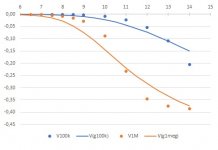
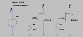
Attached you find a simple test circuit and the results for the gate-source voltage both simmed (lines, V(gxxx)) and measured (dots, Vxxx). The funny resistor values include the DVM-input impedance.
device is Idss 13.9mA
Code:
Vds	V(g1meg)	V1M		V(g100k)	V100k
7,5	-0,0148		-0,0038		-0,0017		-0,0004
8,0	-0,0279		-0,0078		-0,0032		-0,0009
8,5	-0,0478		-0,0160		-0,0057		-0,0017
9,0	-0,0747		-0,0291		-0,0095		-0,0031
10,0	-0,1444		-0,0886		-0,0223		-0,0092
11,0	-0,2188		-0,2330		-0,0437		-0,0228
12,0	-0,2834		-0,3460		-0,0737		-0,0544
13,0	-0,3345		-0,3750		-0,1102		-0,1084
14,0	-0,3737		-0,3860		-0,1497		-0,2050
Attachments
According to my notes that's too much so I made a quick setup to measure it again.... in measurement 100k 10V seems tops (9.2mV).
I took a BF862 with same Idss (13.9mA) and set the Id=10mA (Rs = 10R). With the Vds=10V i measured Vg=3.7mv and 0.6mV with Vds=8.5V.
So, as I said, there is no significant DC voltage at the input of the buffer circuit.
I'm not implying that you made a mistake - it might be that there are differences between the production batches even if the Idss is the same.
Attachments
Anyway these numbers are meaningless because you have to connect your jfet circuit to some signal source or volume pot and those have much lower resistance - 10k volume pot will put this Vg value to much lower value (at max volume it will be less than 1mV and on any other setting even less) so there is no reason to sweat about gate leakage...
If you insist, use lower Vds (by means of cascoding) or use P-channel JFETs, their gates don't leak.
If you insist, use lower Vds (by means of cascoding) or use P-channel JFETs, their gates don't leak.
as i wrote earlier, in a bf862 "turbo" buffer circuit with 2 fet pairs i can tune output dc with a 20k input pot. not nice.
I can have two jfets share the voltage and get spectacular distortion values in simulation.
Are there other ways to cascode a source follower? My attempts to simulate a BJT as cascode all ended in oscillation.
I can have two jfets share the voltage and get spectacular distortion values in simulation.
Are there other ways to cascode a source follower? My attempts to simulate a BJT as cascode all ended in oscillation.
Attachments
Re. you sch. in post #48 - that's not the way to do it. J2 should be some long channel JFET (J310 or similar), R12 is superfluous and R11 is two orders of magnitude too big, etc...
Cascoding with a BJT is non-issue. Working nice since the dawn of time. See here (post #66, buffer sch.) :
http://www.diyaudio.com/forums/pass-labs/244106-lsk-pre-baf-2013-a-2.html#post3682031
Sim can't help you much when you are in the dark about what you are doing. It will help to read about basic stuff (post #60) :
http://www.diyaudio.com/forums/solid-state/301164-mosfet-source-follower-headamp-2.html#post4930339
There's something I am not following here.According to my notes that's too much so I made a quick setup to measure it again.
I took a BF862 with same Idss (13.9mA) and set the Id=10mA (Rs = 10R). With the Vds=10V i measured Vg=3.7mv and 0.6mV with Vds=8.5V.
So, as I said, there is no significant DC voltage at the input of the buffer circuit.
I'm not implying that you made a mistake - it might be that there are differences between the production batches even if the Idss is the same.
If 10mA is flowing through the jFET and the source resistor is 10ohms then there is a voltage of 10mA*10ohms = 100mV across the source resistor.
Where does that 100mV impact on the Vgs of the jFET?
Why are you stating Vg=3.7mv (I note you have no "s" in there)?
It represents the conditions in the circuit under test, the actual buffer. That's the actual Vgs of the input JFET....Where does that 100mV impact on the Vgs of the jFET?
That's the voltage from gate to ground in the actual circuit as a consequence of gate leakage current in the said circuit. Those 3.7mV are measured across the resistor (100k) that connects JFET's gate to ground.Why are you stating Vg=3.7mv (I note you have no "s" in there)?
Last edited:
Does that mean the Vgs = 100mV - 3.7mV = 96.3mVgs?It represents the conditions in the circuit under test, the actual buffer. That's the actual Vgs of the input JFET.
That's the voltage from gate to ground in the actual circuit as a consequence of gate leakage current in the said circuit. Those 3.7mV are measured across the resistor (100k) that connects JFET's gate to ground.
that Vgs seems very high for a high gm device passing 10mA
Last edited:
Cascoding with a BJT is non-issue. Working nice since the dawn of time. See here (post #66, buffer sch.) :
http://www.diyaudio.com/forums/pass-labs/244106-lsk-pre-baf-2013-a-2.html#post3682031
]
I had come that far re BJT cascode in sim, too. Where things blow up is when I add the CFP.
A day in sim saves a week in the workshop...

Not at all if you look at the transfer curve for the BF862 with Idss=13.9mA at Vds=10V....that Vgs seems very high for a high gm device passing 10mA
I told you already, buy some tools and parts, get some real life experience - this aggressive poking in the dark of yours does a lot of harm to those who read your post and think that you know what are you writing about.
Hi,
ElFishi, have You had a look in the DS of the BF862?
There´s a diagram (fig.9?) showing the Gate current as function of drain-gate voltage; typical values at a temperature of 25°C
What You can read from that, diagram is that the gate current shoots up for Vdg > 5V.
Below 5V it ranges around 10^-3nA to 10^-2nA
But at 10V and 10mA its already way up at app. 30nA.
It grows even more with increasing temperature, roughly doubling with every 10°C increase.
Running the JFET wo. a source degeneration resistor at its Idss and at the same applying more than a few Volts Vds it´ll heat up fast.
If there´s now a large gate resistor there will develop a considerable gate voltage.
From a certain point on the process is self-amplifying, leading to latch-up of the JFET which then means that the device is destroyed.
So be careful whith JFETs when following conditions apply:
- high Vdg/Vds
- high Id
- large gate resistor value
- high temperature
I assume, that Your test conditions may already have lead to a latch-up or had come close enough that You could measure considerable gate voltage levels.
As Juma´s test showed ... when You use the JFET cautiously there´ll be no remarkable input offset voltage.
As a rule of thumb, a JFET is ´safe´ as long as You supply with less than 1/4 of its BVgss (Breakdown voltage, specified in DS).
An easy way to have a low-voltage supply is to cascode the JFET.
jauu
Calvin
Thanks Calvin,
I had seen the DS, but I am not sure how to translate Fig 9 to the present case.
It says Vds = 8V and then varies Vdg for fixed Id.
Does this mean Vgs = Vds - Vdg in each graph? If so why would Id stay constant?
V(BR)GSS is given as 20V, your rule suggest to keep Vds under 5V then.
I had seen the DS, but I am not sure how to translate Fig 9 to the present case.
It says Vds = 8V and then varies Vdg for fixed Id.
Does this mean Vgs = Vds - Vdg in each graph? If so why would Id stay constant?
V(BR)GSS is given as 20V, your rule suggest to keep Vds under 5V then.
Does that mean the Vgs = 100mV - 3.7mV = 96.3mVgs?
My question would be answered by stating what the Vgs ended up at.Not at all if you look at the transfer curve for the BF862 with Idss=13.9mA at Vds=10V.
I told you already, buy some tools and parts, get some real life experience - this aggressive poking in the dark of yours does a lot of harm to those who read your post and think that you know what are you writing about.
- Status
- This old topic is closed. If you want to reopen this topic, contact a moderator using the "Report Post" button.
- Home
- Source & Line
- Analog Line Level
- CFP Unity Gain Buffer