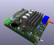
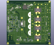
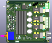
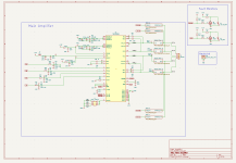
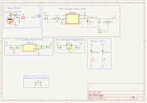
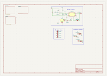
I have worked on TPA3255 based BTL amplifier for a while now. As this is my first time attempting to layout a class D amplifier I would appreciate some feedback.
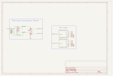
I have tried to follow the layout and schematic from the EVM, the feedback given in other threads on here, as well as SLAA788A for the PFFB, but I have probably missed something.
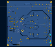
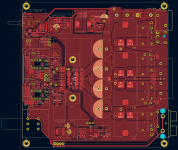
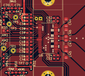
The layout is done on a two layer PCB and I will get all the SMD components assembled by the PCB manufacturer.
The VIA stitching is not done yet, so that is missing. The connectors I have mainly chosen for easy testing.
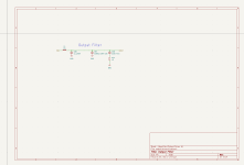
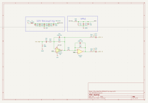
I have attached both schematics and PCB screenshots here, as well as a PDF of the schematic.
Thanks in advance!
I have tried to follow the layout and schematic from the EVM, the feedback given in other threads on here, as well as SLAA788A for the PFFB, but I have probably missed something.
The layout is done on a two layer PCB and I will get all the SMD components assembled by the PCB manufacturer.
The VIA stitching is not done yet, so that is missing. The connectors I have mainly chosen for easy testing.
I have attached both schematics and PCB screenshots here, as well as a PDF of the schematic.
Thanks in advance!
Attachments
-
 side_3d.png150.4 KB · Views: 48
 -
 top_32_no_pth.png144.1 KB · Views: 49
 -
 top_3d.png154.9 KB · Views: 47
 -
TPA3255_pffb_amp.pdf855 KB · Views: 18
-
 pffb.png13.7 KB · Views: 41
 -
 output_filter.png15.5 KB · Views: 40
 -
 main_tpa3255.png54.1 KB · Views: 44
 -
 preamplifier.png26.1 KB · Views: 43
 -
 inputs.png29.3 KB · Views: 39
 -
 power_supply.png41.6 KB · Views: 37
 -
 overall.png27.2 KB · Views: 38
 -
 rear_copper.png66.9 KB · Views: 36
 -
 front_copper.png147.2 KB · Views: 27
 -
 tpa3255_closeup.png122.2 KB · Views: 47