You'll never get 400w RMS out of 37v supply. Without doing the math, it's probably 50w.
For bridge, you get over 300 W.
The driver temperature not being tracked causes some issue. I am studying this effect.
Sorry Guys, I lost this topic for a while but now I am back.
In this matter, people always advice to mount the driver chip on a separate heat sink. I remember the internals of the LME49810 has diodes inside the bias string. Would't it be better to mount the LME49810 on the same heat sink as the output devices to track temp. changes?
If you talk about discrete drivers after the chip, How would you compensate them for temp?
@Tom. So far impressive results for a first attempt! The biggest downside about the STD03's is that you can only use the diode string one way since the side attached to the base is not accessible. This is really pity and because of this you are forced to use difficult tricks to run multiple pairs parallel. If only you could access the diodes string completely (separate from the base) it would be more easy to make a multiple output driver design.
I experiment as well with a pot per pair, but never really got them equal. So I am not really happy with the Sanken advised schematic. I end up with the Arcam way and parallel the diode strings and connect them to one pot. I get decent enough results.
Important to watch is do not exceed the advised 40mA (max 60mA according to Jan Didden). Above 60mA the system will suffer thermal run away and you blow up all devices
 I tried many attempts to bias them in class A but that is not possible with the STD03. In my case everything above 60mA resulted in (longer term) thermal runaway and self-destruction.
Because of above limitations I decided to left the STD03's alone and continue with the ON Thermaltraks. However it has to be said that the sound results once all is working with the STD03's really sublime is, and in line with the very best I've heard.
With kind regards,
Bas
To my knowledge, the LM4702 is basically two LME49811's in one package. I suppose one could connect two in parallel to get higher output current, but I don't really need that. My LME49811 delivers about 8 mA (worst case according to the data sheet is 6.5 mA). So with a worst-case Hfe of the STD03Y that I have, I should have minimum (6.5 mA)*8000 = 52 A output current. Yeah, Hfe depends on collector current (yadda, yadda), but looking at the Hfe curve, I still don't think the amp will be current limited. 52 A is more than the two devices can handle anyway...
The other possible interpretation of your statement, is that you suggest building two power amps using one LM4702. Each power amp would have one pair of STD03's in it. The two amps would then be connected in parallel. This would alleviate separate bias for the two output device pairs, hence, their bias currents could be dialed in to be dead on.
However, with amps in parallel, it is a challenge to ensure that the multiple amp channels share the current evenly. It's not an impossible challenge to solve, but getting accurate load sharing between multiple amps is probably as difficult as getting accurate load sharing between multiple output devices in one amp.
~Tom
I like that approach Tom. I was thinking about it myself too. If you do that you should give each of the two paralleled amplifier stages a own servo to prevent the DC of each stage fight each other. Basically you can follow page 12 of the famous AN-1192 application sheet. http://www.national.com/an/AN/AN-1192.pdf and see one chip side and a pair of STD03's as a whole LM3886.
I think this will be a very convenient different approach to work with chip drivers and the STD03's. Second benefit is that that each chip side has to deliver less current=lower distortion since u share the current demand by both chip sides of the LM4702.
With kind regards,
Bas
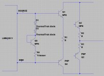
The driver temperature in a double EF output stage shows substantial variation. If its Vbe is not considered in the thermal tracking loop. We will end up over bias. I use the NPN driver connected as diode and insert it in the bias generation. It is attached to the driver heatsink, separated from the ThermalTrak heatsink. The arrangement shows better overall bias thermal tracking performance. I will present test data very soon.If you talk about discrete drivers after the chip, How would you compensate them for temp?
Important to watch is do not exceed the advised 40mA (max 60mA according to Jan Didden). Above 60mA the system will suffer thermal run away and you blow up all devices
According to magazine, Musical Fideility AMS50 is a pure Class A 50 W amp which uses six pairs of STD03 per channel. The bias current per device should be higher than 60 mA.
Attachments
According to magazine, Musical Fideility AMS50 is a pure Class A 50 W amp which uses six pairs of STD03 per channel. The bias current per device should be higher than 60 mA.
Dear Panson,
I know Musical Fidelity is very fond of the STD03's. I know they use +/- 20 STD03's per channel as well in their giant Titan Amplifier. They use them all over the place the last decade started with the former SAP16 devices.
I would die to ever see a schematic from any of those amplifiers, because I am so curious how they manage the Diode string arrangement for Bias. I do know they use just one adjust pot-meter.
Also I am curious how they are able to bias those Sanken's in class A. My own experience is, that is that the diode string inside the sanken's is only accurate till 60mA output bias and not higher. That is also what is stated in Sanken's sheet's. Stubborn as I was I exceed this many times, but then thermal runaway is the result. The diodes don't track good anymore. Of course I can do something wrong, but so far I am not aware.
With kind regards,
Bas
Dear Tom,
Here an example of my working STD03 amplifier design. To obtain more power I use a bridge configuration. Also for driving a subwoofer. This design works still flawless. I am stubborn and tied the diode strings from both pairs together. I stole this from Arcam who does exact the same in their P1 amplifier with two pairs of STD03's.
Ps. The STD49811 can't deliver enough current to fully drive two pairs on STD03's. Better go with the LME49810.
With kind regards,
Bas.
Ps. DC servo not included since this amplifier is used in an active speaker system, where DC is removed in the crossover/input stage
how much is the out put power?
how much is the out put power?
Output power depends on the used and usable voltage rails. The voltage rails should be decided depended on the worst to be expected or required load. Of course with a safe margin and consideration of the SOA of the STD03's and heat sinking enz.
About the DC servo's
Even though care of DC is taken in the crossover stage, Each of the two halve must have a DC servo or a very good DC trimming. This has to do with the fact that each halve has it's own in-depended feedback loop, and will try to fight each others DC offset.
In short, to prevent to both stages keep fighting/correcting each others DC offset a servo is needed for each halve.
With kind regards,
Bas
how much is the out put power?
You can always estimate the output power from the supply rails as, Pout = (Vsupply^2)/(2*Rload).
So for, say, +/-40 V supply and 8 ohm load, you get (40^2)/(2*8) = 1600/16 = 100 W. In reality, you'll probably get more like 90 W as you do lose a little voltage across the output devices and don't drive them completely into saturation.
If you bridge two amplifiers, the total voltage across the load doubles. So for bridged amplifiers, above equation works out to Pout_bridge = ((2*Vsupply)^2)/(2*Rload) = 4*(Vsupply^2)/(2*Rload) = 4*Pout. So if you bridge two 100 W amps, you get 400 W out.
~Tom
In this matter, people always advice to mount the driver chip on a separate heat sink. I remember the internals of the LME49810 has diodes inside the bias string. Would't it be better to mount the LME49810 on the same heat sink as the output devices to track temp. changes?
I don't think that's such a hot idea. That's what I tried first and I had some fairly serious thermal issues that made me rethink the entire design. I ended up redesigning completely as I found the STD03's at about the same time so I don't have data to back up any claims. I can only say that the LME49811+STD03 combo is AWESOME!!
I had mechanical issues mounting the LME49810 to the main heat sink. The DAP (exposed metal on the back) is connected to VEE, hence, needs to be isolated from the heat sink. That turned out to be a royal pain. I used a TO-220 thermal pad to cover the center of the package where the DAP is exposed. That caused the package to crack (!) when I carefully tightened the screws on either end. Then I tried a larger thermal pad that was cut from a large sheet. This material wrinkled below the package and caused it to crack. Thankfully, I had five samples so I did finally make it work by using an aluminum spreader across the drivers and LME49810. I really recommend using the HS335 heat sink that NSC uses in their LME498xx dev kits.
I would expect the tempco of the internal bias of the LME to be designed to allow constant device performance within the specified operating temperature range. This has been done on all chips I've worked on. But I would not expect the chip to be designed with thermal stability in mind when attached to an arbitrary external thermal system as there's no way the designer can know the external thermal system.
@Tom. So far impressive results for a first attempt! The biggest downside about the STD03's is that you can only use the diode string one way since the side attached to the base is not accessible. This is really pity and because of this you are forced to use difficult tricks to run multiple pairs parallel.
Tradeoffs, tradeoffs.... And thank you. Yeah, I'm really quite happy with this amp.
I experiment as well with a pot per pair, but never really got them equal.
If I build the bias circuit with just one pot and the diodes in parallel as you have done, I get about 10~15 % difference between the emitter currents of the two devices. This is caused by device mismatch between the STD03's and the emitter resistors (+/- 5 % tolerance). If I use two separate bias strings, I can tweak it so the transistors' emitter currents are within +/-0.5 % with a little patience. The currents through the two diode strings will differ - probably by the same 10~15 % as with the parallel bias scheme. There is no way they will ever be equal. The voltage across the diodes + pot is the same for the two strings. So if the devices differ slightly, the currents will differ slightly. Ohm's Law in action.
Important to watch is do not exceed the advised 40mA (max 60mA according to Jan Didden). Above 60mA the system will suffer thermal run away and you blow up all devices
What resistance are you using on the emitters? 0.1R? 0.22R? I use 0.22R wire-wound and have no trouble with thermal run-away. I'm running 100 mA per device (200 mA total for the output stage). You've seen my plots for one hour rest after a 60~90-minute run at 100 W. But what I haven't told you is that I've had the amp running for hours daily for the past couple of weeks without issue. I need to upload the latest schematic and results, but work's been busy.
~Tom
Final schematic
Folks,
Attached is the final schematic. I moved the input RF filter to the rear of the input connector. It's the same component values and hook-up as I showed in my first post.
I tried uploading the PCB artwork also, but the .pdf is 1.35 MB, hence, too big for the forum. It's nothing special. I use a star ground topology and fat traces for the output and supplies. I'll upload the file to my website and post a link once I have the page ready.
~Tom
Attachments
How does the performance of ON's Thermaltraks compare to Sanken's? At a fifth to a third of the small quantity price of the STD03s they're certainly interesting despite the much lower hfe.I decided to left the STD03's alone and continue with the ON Thermaltraks. However it has to be said that the sound results once all is working with the STD03's really sublime is, and in line with the very best I've heard.
EDIT: measurements buried in this thread, notably from Doug Self. Haven't spotted any data from a 49811 driving ON parts at typical powers, though. So my question still stands...
Last edited:
Just curious when using the sanken devices in parallel. nothing says that you have to use the internal diodes with every pair. What would happen if you only used one diode string with the first pair and just not use the diodes with the other pairs. When we use multiple pairs of output transistors, one normally only uses one thermal tracking device, presuming that all of the parallel pair devices are close to each other in temperature and current draw. My current Lme project purchased from ebay uses 5 pairs of outputs and as usual one tracking device.
Just curious when using the sanken devices in parallel. nothing says that you have to use the internal diodes with every pair. What would happen if you only used one diode string with the first pair and just not use the diodes with the other pairs.
I've mulled over this quite a bit and tried the various combinations. Here's my thinking: There will be a thermal gradient across the heat sink. The devices closer to the center will probably be warmer than those closer to the ends. So if I was using multiple pairs of output devices but only one diode string, I would use the string from the warmest devices as this will result in the safest bias condition. If several pairs of output devices were used, one could play games like using the diode strings from the "inner" and "outer" devices to get some sort of average reading. I don't think this would be my choice, but it's a possibility.
I tried these biasing schemes in a setup with two pairs of output devices:
1) Two diode strings in parallel, each string having its own bias pot
2) Two diode strings in parallel with one common bias pot
3) One diode string with one bias pot
Option 3) made the quiescent current quite hard to control as the bias current through the diode stack is about 8 mA with a typical LME49811. I did not want to use a resistor across the diode stacks (I believe it's R12 on the schematic -- note that it's marked "open") as this cuts into the amount of base current available for the output devices. I abandoned this setup due to issues getting a reasonably low quiescent current.
Option 2) Works pretty well. The quiescent current (Q current) is fairly easy to adjust, but I'd recommend using a 100R pot rather than the 200R I used as the pot sees the full current through both diode stacks (about 8 mA). So exact adjustment of the Q current is a bit finicky. I ended up with about 10~15 % mismatch in Q current between the two pairs of output devices. Had I matched the emitter resistors and the output devices (both for Vbe and Vf) the mismatch would have been smaller. But 10~15 % is quite decent.
Option 3) is what I ended up using. I like that I have independent control of the Q current for each pair of output devices. This scheme does cause a mismatch of the bias current through the diode stacks as they "see" the same voltage, but have slightly different diode characteristics. The mismatch is on the order of 10~15 % when the Q current in the output devices is trimmed to a mismatch less than +/-0.5 %. But in the end, it's the Q current of the output devices that's the important parameter, which is why I elected to use this biasing scheme.
I did not notice any difference in distortion between options 2) and 3), but I didn't look that hard. In both cases the THD+N for 10-ish W into 8 ohm was well below 0.005 % when running off of a +/-50 V lab supply.
~Tom
How does the performance of ON's Thermaltraks compare to Sanken's? At a fifth to a third of the small quantity price of the STD03s they're certainly interesting despite the much lower hfe.
I looked briefly at ON's TT devices also. I planned to use them as an alternate had I not been able to get the STD03's. Note that the TT diode in ON's devices is NOT on the same die as the BJT. There's quite a bit about the ON Semi devices in Bob Cordell's thread, specifically around post #77.
Having the TT diode on the same DAP as the BJT will obviously help with the thermal tracking. But having the diode fabricated on the same die as the BJT would be even better - same process, good thermal connection, good device matching. The parasitic cap mentioned in the Cordell thread can be dealt with and reduced with proper layout.
Having the diode be completely separate and pinned out separately from the BJT does offer more options as far as the bias circuit goes, though. That's a nice touch of the ON devices.
Note that the ON Semi devices are single BJT's. No darlington here... Hence, the lower Hfe. So you'll need driver transistors. This will make the thermal system more complex.
In the end, the simplicity of the STD03 + LME49811 was overwhelmingly appealing to me. And I was able to get the STD03's at a good price so that, obviously, factored into the equation also.
~Tom
In the end, the simplicity of the STD03 + LME49811 was overwhelmingly appealing to me. And I was able to get the STD03's at a good price so that, obviously, factored into the equation also.
~Tom
Very tempting...
Where to get the STD03?
B&D is one option. Small quantity eBay gets as low as B&D's 50+ unit pricing but I've no insight on whether the eBay parts are genuine.
Yea, verily. Digikey/Newark pricing on the ONs isn't particularly competitive with pricing on the Sankens. It's only if you order directly from ON that the NJL0281D/NJL0302D are $1.93 each.In the end, the simplicity of the STD03 + LME49811 was overwhelmingly appealing to me. And I was able to get the STD03's at a good price so that, obviously, factored into the equation also.
Last edited:
Folks,
Attached is the final schematic. I moved the input RF filter to the rear of the input connector. It's the same component values and hook-up as I showed in my first post.
I tried uploading the PCB artwork also, but the .pdf is 1.35 MB, hence, too big for the forum. It's nothing special. I use a star ground topology and fat traces for the output and supplies. I'll upload the file to my website and post a link once I have the page ready.
~Tom
Very neat Tom,
I don't doubt you the amplifier works great, and I don't want to be the skeptical here, but don't you find it a bit tricky to run the amplifier without any Zobel on the outputs? Did u check for oscillations?
I suggest for extra stability safety margin you mount at least one 5W10R together with 100nF from output to ground.
I build many amplifiers over the years, and without Zobel unexpected by a change of cable type or cable position the amplifier can suddenly start to oscillate.
With kind regards,
Bas
What resistance are you using on the emitters? 0.1R? 0.22R? I use 0.22R wire-wound and have no trouble with thermal run-away. I'm running 100 mA per device (200 mA total for the output stage). You've seen my plots for one hour rest after a 60~90-minute run at 100 W. But what I haven't told you is that I've had the amp running for hours daily for the past couple of weeks without issue. I need to upload the latest schematic and results, but work's been busy.
~Tom
To be honest, I use a low value 0.1R emitter resistor. And in that configuration you really should't get over 60mA. Is logical. I tried higher Re's but for me (based on just listening session's) it never rivals the tight bass I get with 0.1R resistors. I believe you right away higher bias is stable with higher emitter resistors.
With kind regards,
Bas
It's only if you order directly from ON that the NJL0281D/NJL0302D are $1.93 each.
This is volume price. You need to pay $2.9 per device for less than 100 pcs. Better to get free samples.
- Status
- This old topic is closed. If you want to reopen this topic, contact a moderator using the "Report Post" button.
- Home
- Amplifiers
- Chip Amps
- Yet Another LME49811 + STD03 Build