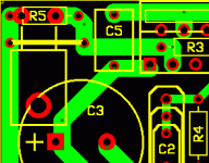
Resistor variation #2
I Don't know if this version is really useful; I made a version of the pcb with the feedback resistor "outside" the chip. This may be useful for the "clean tweakers" willing to experiment with the resistor value without soldering it on the copper side. I don't like the result very much. Please let me know what you think.
Massimo
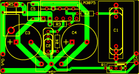
I have been modifying your PCB design for my experimentation ")
this is not finished yet, but you can see some changes i made.
It is smaller.
there is a tiny "protoboard" area for output resistor/inductor experimentation. I like this idea, and i will probably do it for the input as well
the traces are as big as they can be, some are doubled on both sides of the PCB.
resitors can be SMDs or regular resistors.
input traces are thinner which may reduce capacitance where they cross other traces.
you may notice that the Power capacitors are overlapping the other components. this is because i intend them to be on the bottom of the board so they can be strapped to something.
what i will do next is make the board so it can be wired either inverting or non inverting, and possibly add traces for a buffer op-amp which can be optionally used.
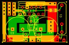
Attachments
- Status
- This old topic is closed. If you want to reopen this topic, contact a moderator using the "Report Post" button.
- Home
- Amplifiers
- Chip Amps
- Yet another GC pcb...