Re: Re: Re: Re: PSU
I just did that already and found nothing about "pole frequency separation between front-end and OPS". The discussion was solely about the OPS itself, H-parameters, you know. Schematics of complete amps (including a front-end) were later published on my website.
Thanks. But wait for my final design. Most people will probably find it ridiculously complex. But who cares, it's DIY, not a commercial project. Also, most hi-end gurus will not be charmed by the concept as I don't shy away from that evil NFB. Again, I really don't care.
As for R2/R3, of course they changed the bias as well. I only referred to them to make clear that these resistors have also an impact on the BW.
I did a quick search on the web, but couldn't find an appropriate entry. So, please, just name a few advantages, only keywords like more headroom etc.
I thought you were a very careful man. So didn't you simmed the circuit before building it? If so, didn't the sim reveal potential problems without C34?
BTW1, to avoid such mistakes as described by you, is precisely the reason for my "obsession with simulations".
BTW2, did you know that Stochino uses gate stoppers ranging from 22 to zero Ohm!?
Frankly speaking, I'm not particular charmed by some of your remarks either. Perhaps we both should change our tone.
Besides, shouldn't you be glad to get also technical feedback, not just (well-deserved) pats.
BTW, I just simmed your OPS (except the protection). The closed loop bandwidth was indeed 10MHz, but the phase shift was quite large: 110 degrees (at that frequency). Also, it peaked about 4dB at 5MHz. The phase margin of the internal FB loop (via R52) was only 40 degrees (@5.2MHz), although the gain margin was much better: 24dB (@36MHz).
THD20 = 30ppm @200W into 4 Ohm. Hmm... a bit more than a measured 20ppm.
How well do the other figures match with your real measurements?
I also looked at the effect of TMC and TPC. They both do almost nothing.
syn08 said:1. Read again.
I just did that already and found nothing about "pole frequency separation between front-end and OPS". The discussion was solely about the OPS itself, H-parameters, you know. Schematics of complete amps (including a front-end) were later published on my website.
2. I was thinking about the fleet of amps on your website rather than those incipient drafts (and BTW, both classic CFB's with unity gain). Anyway nice design - changing the BW (R2, R3) changes the bias as well.
Thanks. But wait for my final design. Most people will probably find it ridiculously complex. But who cares, it's DIY, not a commercial project. Also, most hi-end gurus will not be charmed by the concept as I don't shy away from that evil NFB. Again, I really don't care.
As for R2/R3, of course they changed the bias as well. I only referred to them to make clear that these resistors have also an impact on the BW.
3. Larry Page's Google is a very interesting lecture. Hint: "diamond buffer advantages".
I did a quick search on the web, but couldn't find an appropriate entry. So, please, just name a few advantages, only keywords like more headroom etc.
4. This is an interesting comment. That cap costed me a PCB revision! The prototype was built with only one pair of output devices and no cap was required as long as the diamond buffer current was over 10mA. For whatever reasons, when I was adding more pairs all kind of strange switching effects happened, also depending on the gate stoppers values. Increasing the buffer current was not an option (power dissipation), increasing the gate stopper was also not an option ('cause I was targeting 10MHz unity gain frequency) so here's the cap and BTW, 10nF works fine as well.
I thought you were a very careful man. So didn't you simmed the circuit before building it? If so, didn't the sim reveal potential problems without C34?
BTW1, to avoid such mistakes as described by you, is precisely the reason for my "obsession with simulations".
BTW2, did you know that Stochino uses gate stoppers ranging from 22 to zero Ohm!?
Edmond, unless you radically change your tone I am not willing to continue this discussion, I don't have the time and mood for another mudsling. BTW, I was very confortable on your ignore list.
Frankly speaking, I'm not particular charmed by some of your remarks either. Perhaps we both should change our tone.
Besides, shouldn't you be glad to get also technical feedback, not just (well-deserved) pats.
BTW, I just simmed your OPS (except the protection). The closed loop bandwidth was indeed 10MHz, but the phase shift was quite large: 110 degrees (at that frequency). Also, it peaked about 4dB at 5MHz. The phase margin of the internal FB loop (via R52) was only 40 degrees (@5.2MHz), although the gain margin was much better: 24dB (@36MHz).
THD20 = 30ppm @200W into 4 Ohm. Hmm... a bit more than a measured 20ppm.
How well do the other figures match with your real measurements?
I also looked at the effect of TMC and TPC. They both do almost nothing.
Re: Re: Re: Re: Re: YAP
Ok, Ok, I didn't look thoroughly enough and assumed the OPS was being run open loop.
WRT to C34 maybe the MOSFET input capacitance under severe slewing is being underestimated for some reason?? I dunno.
I’ve encountered the problem driving low fT power BJT’s in the diamond buffer configuration.
To measure it I connected a resistor in series with the collector lead of each driver transistor and monitored the voltage across each with a differential CRO probe (If your CRO has a floating input you can connect the ground clip to the respective supply rail instead).
I got negative spikes in the collector current towards 0mA during rapid slewing (indicating that nearly all the driver transistor emitter current was being taken up by base current to the output device)
This may be a good experiment with your amp, to see if this is the problem or if there is another mechanism at play here WRT to the need for C34?
WRT to home made PCB’s, yes it is a tedious job (I hate it – especially the drilling). For developing I use sodium metasilicate and for etching I use ammonium persulphate at ~60deg C.
Dunno about disposal, I’ve only been collecting the stuff thus far. A good question though. I need to ask where we get rid of it at work.
Cheers,
Glen
syn08 said:
Thanks Glen,
Well, that's about half the THD20 performance of the PGP. 2ppm vs. 1ppm but if you are happy with a slight (10-15%) overshoot, the THD20 can be easily brought down to 1ppm.
That's my common understanding about C34 as well. However, without C34, in multiple output devices configuration, the amp was unstable during high speed transients (smeared traces on a 350MHz scope). This is better analyzed in terms of charge rather than current and 10mA over 250nS (which is the rise/fall time in this amp) ought to be enough to provide the required MOSFET gate charges without any cap.
And you are finalizing your project when the winter is almost gone? I though you were planning to replace your home heating system?
Not a problem to buy all those tools... Are you aware of any store with Time on sale? I could also use a new pair of eyes and some patience.
Edit: Just curious, what are you using for etching the PCBs and how are you disposing the used chemicals?
Ok, Ok, I didn't look thoroughly enough and assumed the OPS was being run open loop.
WRT to C34 maybe the MOSFET input capacitance under severe slewing is being underestimated for some reason?? I dunno.
I’ve encountered the problem driving low fT power BJT’s in the diamond buffer configuration.
To measure it I connected a resistor in series with the collector lead of each driver transistor and monitored the voltage across each with a differential CRO probe (If your CRO has a floating input you can connect the ground clip to the respective supply rail instead).
I got negative spikes in the collector current towards 0mA during rapid slewing (indicating that nearly all the driver transistor emitter current was being taken up by base current to the output device)
This may be a good experiment with your amp, to see if this is the problem or if there is another mechanism at play here WRT to the need for C34?
WRT to home made PCB’s, yes it is a tedious job (I hate it – especially the drilling). For developing I use sodium metasilicate and for etching I use ammonium persulphate at ~60deg C.
Dunno about disposal, I’ve only been collecting the stuff thus far. A good question though. I need to ask where we get rid of it at work.
Cheers,
Glen
I'm currently looking a bit at Diamond buffers and interestingly they're always driven from a single signal using a NPN and a PNP as phase splitter.
Maybe the only reason for this is that usually only the standard LTP is used.
However if one uses a complementary differential pair, thus already has 2 signals of opposite phase, it seems straightforward to use a NPN only-diamond buffer.
Is that reasonable or am I just running low on coffeine?
I'm just asking, since I've never seen such a thing yet.
Have fun, Hannes
PS: etching, drilling your own boards has my full respect...I prefer to send the layout to a cheap board house
Re: Re: Re: Re: Re: PSU
1. Already count me in. I don't have a problem with complexity per se (parts cost almost nothing today) but with manageability. As I already mentioned, melting 100 trannies in a single block with 37.4 feedback loops that are kept together by simulation glue is not appealing to me and I don't want to go on that path. Rather than that, I want to design, build and use a set of well characterized building blocks, that can be combined like a LEGO.
2. Start from Walt Jung original articles.
http://waltjung.org/PDFs/WTnT_Op_Amp_Audio_1.pdf
http://waltjung.org/PDFs/WTnT_Op_Amp_Audio_2.pdf
then build your way up to the BUF634 design. You already mentioned two advantages, I added another one (before using the diamond buffer distortion were increasing with increasing the output device quiescent current) and here's another one: stability. With a simple follower, the whole OPS was slightly unstable for fast transients. Only C34 did not solve the problem... I haven't looked closely at this, but I suspect it's about how the MOSFET input impedance (buffer load) is reflected at the buffer input.
3. Don't worry, I simmed it. I only don't want to talk about simulation results; as you know, our simulations never matched to a degree that would make a discussion consistent. Honestly, as long as I don't trust my simulations more than I trust yours, I don't care much why. You think PSpice is a piece of crap, I don't have any plans to switch to anything else as long as I have a perpetual licence and free upgrades for a suite that allows me to own the whole chain from electrical design to PCB Gerbers outputs.
4. I have mentioned some preliminary results in another post here:
http://www.diyaudio.com/forums/showthread.php?postid=1569957#post1569957
Since then I tweaked the thing a little, so there are some changes. Closed loop bandwidth is still 8MHz and the phase shift is 95 degrees. With 220ohm/390pF at the input and the Zoebel + coil in place, the rise and fall times are 250nS symmetrical. At 1KHz a 80Vvv square wave renders a slew rate of about 300V/us. You have a preliminary sample of the reactive load response here:
http://www.diyaudio.com/forums/showthread.php?postid=1575583#post1575583
5. In both my simulations and experiments, there is a huge difference between a simple Miller cap and TPC. It's only TMC that does nothing compared to TPC.
Honestly, I don't understand why a gain of 1.3 would trigger a vast TMC improvement over a gain of 1. OTOH, if there are certain topologies and configuration where TMC has a significant advantage over TPC, this is worth an in depth study for which simulation is the ideal tool. You may want to revisit this topic and let everybody know about.
Edit: Unfortunately I lost another auction for a HP8751A that would let me measure the loop gain. These 15 years old things sell like crazy...
Edmond Stuart said:
1. Most people will probably find it ridiculously complex...
2. I did a quick search on the web, but couldn't find an appropriate entry. So, please, just name a few advantages, only keywords like more headroom etc.
3. I thought you were a very careful man. So didn't you simmed the circuit before building it? If so, didn't the sim reveal potential problems without C34?
4. BTW, I just simmed your OPS (except the protection). The closed loop bandwidth was indeed 10MHz, but the phase shift was quite large: 110 degrees (at that frequency). Also, it peaked about 4dB at 5MHz. The phase margin of the internal FB loop (via R52) was only 40 degrees (@5.2MHz), although the gain margin was much better: 24dB (@36MHz).
THD20 = 30ppm @200W into 4 Ohm. Hmm... a bit more than a measured 20ppm.
How well do the other figures match with your real measurements?
5. I also looked at the effect of TMC and TPC. They both do almost nothing.
1. Already count me in. I don't have a problem with complexity per se (parts cost almost nothing today) but with manageability. As I already mentioned, melting 100 trannies in a single block with 37.4 feedback loops that are kept together by simulation glue is not appealing to me and I don't want to go on that path. Rather than that, I want to design, build and use a set of well characterized building blocks, that can be combined like a LEGO.
2. Start from Walt Jung original articles.
http://waltjung.org/PDFs/WTnT_Op_Amp_Audio_1.pdf
http://waltjung.org/PDFs/WTnT_Op_Amp_Audio_2.pdf
then build your way up to the BUF634 design. You already mentioned two advantages, I added another one (before using the diamond buffer distortion were increasing with increasing the output device quiescent current) and here's another one: stability. With a simple follower, the whole OPS was slightly unstable for fast transients. Only C34 did not solve the problem... I haven't looked closely at this, but I suspect it's about how the MOSFET input impedance (buffer load) is reflected at the buffer input.
3. Don't worry, I simmed it. I only don't want to talk about simulation results; as you know, our simulations never matched to a degree that would make a discussion consistent. Honestly, as long as I don't trust my simulations more than I trust yours, I don't care much why. You think PSpice is a piece of crap, I don't have any plans to switch to anything else as long as I have a perpetual licence and free upgrades for a suite that allows me to own the whole chain from electrical design to PCB Gerbers outputs.
4. I have mentioned some preliminary results in another post here:
http://www.diyaudio.com/forums/showthread.php?postid=1569957#post1569957
Since then I tweaked the thing a little, so there are some changes. Closed loop bandwidth is still 8MHz and the phase shift is 95 degrees. With 220ohm/390pF at the input and the Zoebel + coil in place, the rise and fall times are 250nS symmetrical. At 1KHz a 80Vvv square wave renders a slew rate of about 300V/us. You have a preliminary sample of the reactive load response here:
http://www.diyaudio.com/forums/showthread.php?postid=1575583#post1575583
5. In both my simulations and experiments, there is a huge difference between a simple Miller cap and TPC. It's only TMC that does nothing compared to TPC.
Honestly, I don't understand why a gain of 1.3 would trigger a vast TMC improvement over a gain of 1. OTOH, if there are certain topologies and configuration where TMC has a significant advantage over TPC, this is worth an in depth study for which simulation is the ideal tool. You may want to revisit this topic and let everybody know about.
Edit: Unfortunately I lost another auction for a HP8751A that would let me measure the loop gain. These 15 years old things sell like crazy...
Re: Re: Re: Re: Re: Re: PSU
@1. Although your Lego approach has appeal in its own right, for optimal results both parts (FE and OPS) have to be carefully tuned to each other. I don't think that's possible with 'of the self' PCBs, that is, PCBs made for one project and then used for another. Unless of course, you have already taken future modifications into consideration. Not an easy task.
100 trannies? only a lousy 70
37.4? only two in the signal path, 3 bias loops and one 'active clamp' loop.
As for 'manageability', you have a point and as a matter of fact, I was already thinking of how I can split the boards into smaller parts.
@2. Regrettably, the Walt Jung papers didn't give much insight into your specific problem with fast transient, as it deals only with (small) BJTs. Never mind. I think that the problem stems from the fact that at large excursions, Cgd of the 'top' respectively the 'bottom' MOSFETs becomes very unequal. As a result, the turn-on time will be much faster than the turn-off (of the other MOSFETs) with a traditional driver stage and one will have a potential problem. With your topology it's quite the opposite and no issues with cross-conduction, right?
@3. Come on, please don't make such a fuss about nothing. Indeed, three times there were serious discrepancies and all three can be explained (netlist error, different models, that I discovered later and one careless simulation). Besides, just because I don't trust my sims 100%, just as as you do, it's interesting to compare results, also with real measurements. We both can learn from this.
Regarding your amp, because you have simulated it, may I conclude that your sim did NOT reveal the problems related to C34 and the driver stage? (otherwise a PCB redesign was not necessary)
@4. The step response looks okay, taken into account that the ringing is caused by the Zoebel* network. I'm amazed about the large slew rate. Great!
@5. Weird but interesting. If results are so different, it's certainly worthwhile to have a closer look at this issue. You know, TMC is one of my little babies. As soon as I have found out what's going on, I'll let you know.
As for the gain of 1 vs. 1.3, forget it; it was only a wild guess.
@HP8751A. Can this nice piece of equipment also be use to measure an internal response of a Miller loop? If so that would be great.
* Sorry Brian, I mean Zobel
syn08 said:1. Already count me in. I don't have a problem with complexity per se (parts cost almost nothing today) but with manageability. As I already mentioned, melting 100 trannies in a single block with 37.4 feedback loops that are kept together by simulation glue is not appealing to me and I don't want to go on that path. Rather than that, I want to design, build and use a set of well characterized building blocks, that can be combined like a LEGO.
2. Start from Walt Jung original articles.
http://waltjung.org/PDFs/WTnT_Op_Amp_Audio_1.pdf
http://waltjung.org/PDFs/WTnT_Op_Amp_Audio_2.pdf
then build your way up to the BUF634 design. You already mentioned two advantages, I added another one (before using the diamond buffer distortion were increasing with increasing the output device quiescent current) and here's another one: stability. With a simple follower, the whole OPS was slightly unstable for fast transients. Only C34 did not solve the problem... I haven't looked closely at this, but I suspect it's about how the MOSFET input impedance (buffer load) is reflected at the buffer input.
3. Don't worry, I simmed it. I only don't want to talk about simulation results; as you know, our simulations never matched to a degree that would make a discussion consistent. Honestly, as long as I don't trust my simulations more than I trust yours, I don't care much why. You think PSpice is a piece of crap, I don't have any plans to switch to anything else as long as I have a perpetual licence and free upgrades for a suite that allows me to own the whole chain from electrical design to PCB Gerbers outputs.
4. I have mentioned some preliminary results in another post here:
http://www.diyaudio.com/forums/showthread.php?postid=1569957#post1569957
Since then I tweaked the thing a little, so there are some changes. Closed loop bandwidth is still 8MHz and the phase shift is 95 degrees. With 220ohm/390pF at the input and the Zoebel + coil in place, the rise and fall times are 250nS symmetrical. At 1KHz a 80Vvv square wave renders a slew rate of about 300V/us. You have a preliminary sample of the reactive load response here:
http://www.diyaudio.com/forums/showthread.php?postid=1575583#post1575583
5. In both my simulations and experiments, there is a huge difference between a simple Miller cap and TPC. It's only TMC that does nothing compared to TPC.
Honestly, I don't understand why a gain of 1.3 would trigger a vast TMC improvement over a gain of 1. OTOH, if there are certain topologies and configuration where TMC has a significant advantage over TPC, this is worth an in depth study for which simulation is the ideal tool. You may want to revisit this topic and let everybody know about.
Edit: Unfortunately I lost another auction for a HP8751A that would let me measure the loop gain. These 15 years old things sell like crazy...
@1. Although your Lego approach has appeal in its own right, for optimal results both parts (FE and OPS) have to be carefully tuned to each other. I don't think that's possible with 'of the self' PCBs, that is, PCBs made for one project and then used for another. Unless of course, you have already taken future modifications into consideration. Not an easy task.
100 trannies? only a lousy 70
37.4? only two in the signal path, 3 bias loops and one 'active clamp' loop.
As for 'manageability', you have a point and as a matter of fact, I was already thinking of how I can split the boards into smaller parts.
@2. Regrettably, the Walt Jung papers didn't give much insight into your specific problem with fast transient, as it deals only with (small) BJTs. Never mind. I think that the problem stems from the fact that at large excursions, Cgd of the 'top' respectively the 'bottom' MOSFETs becomes very unequal. As a result, the turn-on time will be much faster than the turn-off (of the other MOSFETs) with a traditional driver stage and one will have a potential problem. With your topology it's quite the opposite and no issues with cross-conduction, right?
@3. Come on, please don't make such a fuss about nothing. Indeed, three times there were serious discrepancies and all three can be explained (netlist error, different models, that I discovered later and one careless simulation). Besides, just because I don't trust my sims 100%, just as as you do, it's interesting to compare results, also with real measurements. We both can learn from this.
Regarding your amp, because you have simulated it, may I conclude that your sim did NOT reveal the problems related to C34 and the driver stage? (otherwise a PCB redesign was not necessary)
@4. The step response looks okay, taken into account that the ringing is caused by the Zoebel* network. I'm amazed about the large slew rate. Great!
@5. Weird but interesting. If results are so different, it's certainly worthwhile to have a closer look at this issue. You know, TMC is one of my little babies. As soon as I have found out what's going on, I'll let you know.
As for the gain of 1 vs. 1.3, forget it; it was only a wild guess.
@HP8751A. Can this nice piece of equipment also be use to measure an internal response of a Miller loop? If so that would be great.
* Sorry Brian, I mean Zobel
Re: Re: Re: Re: Re: Re: Re: PSU
1. Yes, absolutely no problem.
2. No, I have not noticed any issues in simulations with C34. However, my sims were not as extended as yours. I had myself some convergence issues in the LM285-2.5 and -1.2 subckt (this model always creates problems in sims) so I had to replace them with DC sources. Also I did not AC and TRAN sim with the protection in place. And a few other simplifications... The K1530/J201 device models are Andy's.
3. 8751A can do whatever one may wish in 5Hz-500MHz, provided you have the right accessories and find proper ways to break the loop. The three inputs (Reference, A and B) are all floating.
Edmond Stuart said:
1. With your topology it's quite the opposite and no issues with cross-conduction, right?
2. Regarding your amp, because you have simulated it, may I conclude that your sim did NOT reveal the problems related to C34 and the driver stage? (otherwise a PCB redesign was not necessary)
3. @HP8751A. Can this nice piece of equipment also be use to measure an internal response of a Miller loop? If so that would be great.
1. Yes, absolutely no problem.
2. No, I have not noticed any issues in simulations with C34. However, my sims were not as extended as yours. I had myself some convergence issues in the LM285-2.5 and -1.2 subckt (this model always creates problems in sims) so I had to replace them with DC sources. Also I did not AC and TRAN sim with the protection in place. And a few other simplifications... The K1530/J201 device models are Andy's.
3. 8751A can do whatever one may wish in 5Hz-500MHz, provided you have the right accessories and find proper ways to break the loop. The three inputs (Reference, A and B) are all floating.
TPC vs. TMC
Common sense (and theory) tells us that TPC (two pole compensation) reduces both the distortion of front-end and OPS as well, while TMC (transitional Miller compensation) reduces only the distortion of the OPS. So one may wonder why using TMC at all. The point is that the phase response of TMC is much better (TPC shows a nasty dip). Since -generally!- the OPS contributes the most to distortion, little is gained by a further distortion reduction of the front-end. In this regard, TPC has no advantage over TMC, it only spoils the phase response, resulting in overshoot. So far so good.
Back to YAP. Ovidiu reported: "In both my simulations and experiments, there is a huge difference between a simple Miller cap and TPC. It's only TMC that does nothing compared to TPC. "
Hmm.... at first glance rather weird I thought. Later on, I realized that it only makes sense if the OPS is NOT the main contributor to distortion. Was that really the case? According to my sims, definitely yes!
I've simmed two circuits (TMC or TPC disabled): one with ideal and distortionless components in the front-end and one with such components in the output stage. Et voilà..... THD20 of the first one was 9ppm, while the other one produced 30ppm! So most of the distortion stems from the front-end, making TMC ineffective.
syn08 said:[snip]
In both my simulations and experiments, there is a huge difference between a simple Miller cap and TPC. It's only TMC that does nothing compared to TPC.
............... if there are certain topologies and configuration where TMC has a significant advantage over TPC, this is worth an in depth study for which simulation is the ideal tool. You may want to revisit this topic and let everybody know about.
[snip]
Common sense (and theory) tells us that TPC (two pole compensation) reduces both the distortion of front-end and OPS as well, while TMC (transitional Miller compensation) reduces only the distortion of the OPS. So one may wonder why using TMC at all. The point is that the phase response of TMC is much better (TPC shows a nasty dip). Since -generally!- the OPS contributes the most to distortion, little is gained by a further distortion reduction of the front-end. In this regard, TPC has no advantage over TMC, it only spoils the phase response, resulting in overshoot. So far so good.
Back to YAP. Ovidiu reported: "In both my simulations and experiments, there is a huge difference between a simple Miller cap and TPC. It's only TMC that does nothing compared to TPC. "
Hmm.... at first glance rather weird I thought. Later on, I realized that it only makes sense if the OPS is NOT the main contributor to distortion. Was that really the case? According to my sims, definitely yes!
I've simmed two circuits (TMC or TPC disabled): one with ideal and distortionless components in the front-end and one with such components in the output stage. Et voilà..... THD20 of the first one was 9ppm, while the other one produced 30ppm! So most of the distortion stems from the front-end, making TMC ineffective.
Re: TPC vs. TMC
I'm afraid I don't really follow. Care to post the schematics you used? Thanks.
Edmond Stuart said:
I've simmed two circuits (TMC or TPC disabled): one with ideal and distortionless components in the front-end and one with such components in the output stage. Et voilà..... THD20 of the first one was 9ppm, while the other one produced 30ppm! So most of the distortion stems from the front-end, making TMC ineffective.
I'm afraid I don't really follow. Care to post the schematics you used? Thanks.
Re: Re: TPC vs. TMC
Of course I could post the schematics, although extra work to make them 'publishable'. Moreover, as you are not familiar with specific MicroCap symbols (I suppose), this might lead to even more questions. So I think it should be more efficient if you clarify what exactly you don't understand. But I guess you have some trouble with the meaning of "ideal and distortionless components", right?
These are, using MicroCap terminology, so called "dependent sources".
In the first schematic, I've replaced the BJTs by "current-controlled current sources" and gain of 1000, except in case of the current mirrors+cascodes, then the gain is of course just 1
In the other schematic, I have replaced the MOSFETs by "voltage-controlled voltage sources" with a gain of 1.
That's all. If you have more or other questions, please, let me know.
BTW, what about my question which you can find here: http://www.diyaudio.com/forums/showthread.php?postid=1595502#post1595502
syn08 said:I'm afraid I don't really follow. Care to post the schematics you used? Thanks.
Of course I could post the schematics, although extra work to make them 'publishable'. Moreover, as you are not familiar with specific MicroCap symbols (I suppose), this might lead to even more questions. So I think it should be more efficient if you clarify what exactly you don't understand. But I guess you have some trouble with the meaning of "ideal and distortionless components", right?
These are, using MicroCap terminology, so called "dependent sources".
In the first schematic, I've replaced the BJTs by "current-controlled current sources" and gain of 1000, except in case of the current mirrors+cascodes, then the gain is of course just 1
In the other schematic, I have replaced the MOSFETs by "voltage-controlled voltage sources" with a gain of 1.
That's all. If you have more or other questions, please, let me know.
BTW, what about my question which you can find here: http://www.diyaudio.com/forums/showthread.php?postid=1595502#post1595502
TPC vs. TMC
In the meantime I realized that there may be mores sources of confusion, like using the word 'front-end'. By this I mean the drivers and pre-drivers (and not the circuit around the op-amps). Also the term OPS may lead to confusion. By this I mean the power MOSFET stage.
All together, enough reason to post at least one of the schematics. I hope I have taken away any confusion now.
Notice that I too have tweaked the compensation to lower the BW to 8MHz, not that it really matters, as the purpose of this exercise was to pinpoint the main sources of distortion. As it seems, these are the drivers and/or the pre-drivers, so not the MOSFET stage. If that's indeed the case, then this explains why TMC (opposed to TPC) has no advantage at all.
BTW, Douglas Self told me once he didn't get excited (his words) about TMC. I'm pretty sure that also in his case the effect of TMC was swamp by other kinds of (non-OPS) distortions.
Attachments
Re: Re: Re: TPC vs. TMC
Yes, that concept of "distortionless" was unclear to me. I understand now... I still have some difficulties in understanding why the front end may have more distortions than the OPS, I'll take a closer look myself.
I'm not sure I understand your question about the LT1166, could you clarify what is the behaviour you noticed?
Edmond Stuart said:
Of course I could post the schematics, although extra work to make them 'publishable'. Moreover, as you are not familiar with specific MicroCap symbols (I suppose), this might lead to even more questions. So I think it should be more efficient if you clarify what exactly you don't understand. But I guess you have some trouble with the meaning of "ideal and distortionless components", right?
BTW, what about my question which you can find here: http://www.diyaudio.com/forums/showthread.php?postid=1595502#post1595502
Yes, that concept of "distortionless" was unclear to me. I understand now... I still have some difficulties in understanding why the front end may have more distortions than the OPS, I'll take a closer look myself.
I'm not sure I understand your question about the LT1166, could you clarify what is the behaviour you noticed?
Thanks for explaning the abbr.'s I was just thinking wth. is it about this forum and the shortening of words and phrases hehe :-D.
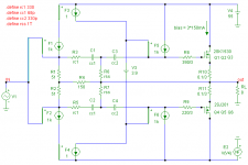
Oh well I'll get to the point, when looking at ops.gif I'm thinking one might try a low value resistor like a few ohms between emitter of q28 and collector of q18 and of course on the other side too, I'm not sure how it will work in your circuit but it helped one of mine, It's a little bit similar, but I'm not using current feeeedback and you use fancy things like constant current sources and overload protection and stuff hehe.. btw, thats a nice overload protection.. :-D.. Kind of almost shut's the whole thing down does it?
The circuit looks nice to me, that's almost like I'd like to make an amp some day, but with fewer components if possible..
Hmm well' I'm not sure about simulation of thd, the lowest I got was 6e-06% at 50w in multisim with an almost normal complementary , balanced circuit with follower output,but at least it gives a picture of the relative level I guess , and the levels at different frequencies are always nice to see.
Ovidiu, congrats on an explendid amplifier project! 
When you were talking about some of the problems you saw when increasing the number of parallel output devices, it made me wonder what the output impedance of the drivers looks like vs frequency. It would be interesting to see what would happen in the simulator by replacing the output stage by a unity gain VCVS, adding a monster sized inductor in series with the global feedback resistor, then injecting an AC current into the driver outputs to look at ZOUT(driver) vs freq.
When you were talking about some of the problems you saw when increasing the number of parallel output devices, it made me wonder what the output impedance of the drivers looks like vs frequency. It would be interesting to see what would happen in the simulator by replacing the output stage by a unity gain VCVS, adding a monster sized inductor in series with the global feedback resistor, then injecting an AC current into the driver outputs to look at ZOUT(driver) vs freq.
nikwal said:Thanks for explaning the abbr.'s I was just thinking wth. is it about this forum and the shortening of words and phrases hehe :-D.
Kind of almost shut's the whole thing down does it?
It does a controlled shutdown, that is, it shuts down the current through the driver and the VAS in a certain sequence, to avoid the output to swing to the rails under fault conditions.
space2000 said:hi syn08,
how easy will be to make this amp? its looks not so easy.
does it needs to make both sided trace pcb?
thanks.
It's not for beginners. Yes, you need two side PCBs. Gerbers will be available on my web site.
Hi,
nice abbreviations you are using here.
I fully agree, the OPC does sufficiently severe damage so why make things even worse by TPC.
The OPC, OPS, TPC, TMC or whatever phase compensation does not reduce any distortion in the IPS, OPS or anywhere. It does only create a series of nasty sounding distortions in several ways.
Lumba Ogir said:
The OPC, OPS, TPC, TMC or whatever phase compensation does not reduce any distortion in the IPS, OPS or anywhere. It does only create a series of nasty sounding distortions in several ways.
:bs: :bs: :bs: :bs: :bs: :bs: :bs: :bs: :bs: :bs: :bs: :bs: :bs: :bs:
Sweet ignorance...
- Status
- This old topic is closed. If you want to reopen this topic, contact a moderator using the "Report Post" button.
- Home
- Amplifiers
- Solid State
- YAP - Yet Another PowerAmp