Attached is my *.asc file - have a play.
Hi Glen,
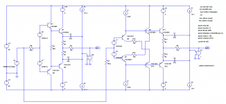
I had a look at this simulation. One thing I saw was that ".options plotwinsize 0" wasn't included. Did you turn compression off via the menus? I stopped doing that after I found out the setting doesn't stick when shutting down LTspice and starting it up again. Anyway, I added that. The other thing I did was to make ideal current mirrors with CCCS'es and used an ideal unity gain VCVS for the output stage. I set up Miller compensation with similar values to YAP, but without TMC, and made a CFB buffer out of each one. For the diamond buffer, I set each shunt voltage source to one-half the nominal voltage of the LM385-1.2. Then I found the bias current in Q11 and Q12, and set the shunt voltages for the cascaded EF to make the bias currents in Q1 and Q2 the same as Q11 and Q12. I made the simulation 12 cycles and used my usual macros for setting up the time step. I added source resistors which can be changed by adjusting the ".param RS 100" directive.
What I found is that with Rs set to a near-zero value, distortion was very low and for all practical purposes identical for the two circuits. With Rs = 100, the cascaded EF had about 1.6x the distortion of the diamond buffer. I don't know if this makes any difference in the real world, as one would expect output stage distortion to dominate anyway.
This did make me wonder about an unrelated topic, namely the output impedance of the "main" (not OPS) VAS when TMC is used. I expect this to be higher than for straight Miller comp, but I need to go back to my main sims to test that. Anyway, I've attached a picture of the schematic below, as well as a zip file containing the LTspice simulation file and model files. I'm still a bit baffled by what you saw with the distortion of the collector currents.
Attachments
Hi Glen,
I had a look at this simulation.
Now it makes some sense...
One of the questions that remained unanswered is about the impact of the diamond buffer folowwing the VAS. If you recall, it was stability that asked for this type of buffer vs. a simple EF.
I never had time for a throughout analysis, but one of the possible reasons for better stability is the way the diamond buffer mirros it's load.
The load of this buffer is essentially capacitive (namely Ciss of the output MOSFETs). A classic EF stage will have a load impedance pole at a frequency of Fp= 1/2*PI*Re*Ciss where Re is the EF emitter resistor. Taking Re=100ohm and Ciss=3.5nF (for 4xMOSFET devices) the pole is at a frequency of 450KHz. The input impedance of the EF is beta times larger and this impedance loads the VAS. When closing the loop, this load impedance pole travels God knows where and perhaps it may travel to places we would not like it to be...
Now, if Re is very large, as for the diamond buffer (that has CCSs instead of emitter resistors), the load pole remains practically in the origin. The input impedance of the diamond buffer (loading the VAS) is approximatively Ciss/beta (in particular if the buffer current is large, so that rbe is small). This is 20-30pF only...
Bottom line, it seems to me that the CCS diamond EF better isolates the VAS from the large, nonlinear, output MOSFETs Ciss. And, interesting enough, the Jeff Rowland M-9 amp chosed the same solution for the buffer, in 1992.
One thing I saw was that ".options plotwinsize 0" wasn't included. Did you turn compression off via the menus?
I'm still a bit baffled by what you saw with the distortion of the collector currents.
Hi Andy.
Yes, I always manually turn off the compression. Maybe I didn't explain the collector current distortion thing very well; but I do not think there is anything unusual here though.
Just sim the input stage buffer with, say a full scale sinewave input voltage at 20kHz and no load and you will see some quite horrible and substantial ac collector currents.
This is a substantial source of distortion (which is not relieved by bootstrapping the pre-driver transistors) and is a symptom of the large voltage swing at the input stage.
The best way top combat this issue (that I've found, anyway) is to run the CFB OPS with a significant gain (say X5) to reduce the collector voltage swing on the input transistors.To compensate for the lower loop gain (caused by the higher closed loop gain) I do not use a 1:1 current mirror VAS. In fact, I use a emitter follower buffered VAS with a resistive load on the input stage of around 1k (this does make frequency compensation of miller loop necessary though). Also, this way, I don't need to run the input stage so hot either, which seems to give better linearity results too (input stage has a bias current of 2.5mA, while I can set the VAS standing current to any thing I want, independantly.
Anyway, can't eleborate much more now as I've gotta go for a day or two. See ya.......
Last edited:
Glen,
This sounds interesting. I'd definitely like to hear more about it. Since it's not specifically about YAP, maybe we could continue this discussion in a more general thread about CFB output stages. That subject could make for a good thread I think.
OK Andy, maybe in the future (Not snubbing you or anything - I really have too many other things that I should be doing
") )
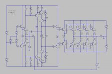
)My intrastate job got called off at the last minute so here I am again today. One last post here: Attached is a bare-bones schematic of my basic CFB OPS using the ideas which I have found (or think) to work best.
This version is scaled to deliver 50W in 4 ohms in class A (I’m actually building this one ATM). The OPS has a closed loop gain of 5. Without any TPC or TMC and a very manageable ULGF of only 2MHz, its 50W/4-ohm THD-20 sims in isolation as follows:
Harmonic Frequency Fourier Normalized Phase Normalized
Number [Hz] Component Component [degree] Phase [deg]
1 2.000e+04 1.998e+01 1.000e+00 -0.47° 0.00°
2 4.000e+04 1.162e-04 5.817e-06 -58.90° -58.43°
3 6.000e+04 2.261e-04 1.132e-05 88.54° 89.01°
4 8.000e+04 3.875e-06 1.939e-07 -91.82° -91.35°
5 1.000e+05 3.539e-05 1.771e-06 -78.70° -78.23°
6 1.200e+05 1.372e-06 6.865e-08 118.01° 118.48°
7 1.400e+05 7.260e-06 3.633e-07 108.67° 109.14°
8 1.600e+05 4.124e-07 2.064e-08 -61.31° -60.85°
9 1.800e+05 1.520e-06 7.607e-08 -65.27° -64.80°
Total Harmonic Distortion: 0.001285%
I’m using TPC in the final version, and coupling it to the modified TPC “Blameless” frontend that I described in that other thread a while ago.
The input stage distortion is effectively minimised by the reduced voltage swing; and don’t underestimate the linearity benefit of only needing 1/5 the voltage swing from the frontend! (Another trick I use here is to not lower the front end voltage rails accordingly).
Anyway, this basic CFB OPS augmented with TPC and coupled to my version of the “Blameless” frontend sims waaay under 1ppm THD-20, and is still a relatively simple design.
Cheers,
Glen
Attachments
Last edited:
OK, one last post ; here is the (not much worse) optimal class-B (50W/4 ohms) THD-20 result (still just straight Miller comp and a 2MHz ULGF).
I'm just posting this before some one tells me that I'm cheating by posting class A results. In reality, class A does not guarantee hugely improved linearity at full power. (Of course, the performance gap is much wider as the power level is reduced, however).
Harmonic Frequency Fourier Normalized Phase Normalized
Number [Hz] Component Component [degree] Phase [deg]
1 2.000e+04 1.998e+01 1.000e+00 -0.46° 0.00°
2 4.000e+04 2.862e-05 1.432e-06 -33.90° -33.43°
3 6.000e+04 3.460e-04 1.731e-05 91.32° 91.78°
4 8.000e+04 3.646e-05 1.825e-06 128.95° 129.41°
5 1.000e+05 7.785e-05 3.896e-06 73.22° 73.68°
6 1.200e+05 2.919e-05 1.461e-06 122.04° 122.51°
7 1.400e+05 1.201e-04 6.012e-06 91.75° 92.21°
8 1.600e+05 1.551e-05 7.764e-07 128.34° 128.80°
9 1.800e+05 1.051e-04 5.261e-06 88.07° 88.54°
Total Harmonic Distortion: 0.001967%
; here is the (not much worse) optimal class-B (50W/4 ohms) THD-20 result (still just straight Miller comp and a 2MHz ULGF).I'm just posting this before some one tells me that I'm cheating by posting class A results. In reality, class A does not guarantee hugely improved linearity at full power. (Of course, the performance gap is much wider as the power level is reduced, however).
Harmonic Frequency Fourier Normalized Phase Normalized
Number [Hz] Component Component [degree] Phase [deg]
1 2.000e+04 1.998e+01 1.000e+00 -0.46° 0.00°
2 4.000e+04 2.862e-05 1.432e-06 -33.90° -33.43°
3 6.000e+04 3.460e-04 1.731e-05 91.32° 91.78°
4 8.000e+04 3.646e-05 1.825e-06 128.95° 129.41°
5 1.000e+05 7.785e-05 3.896e-06 73.22° 73.68°
6 1.200e+05 2.919e-05 1.461e-06 122.04° 122.51°
7 1.400e+05 1.201e-04 6.012e-06 91.75° 92.21°
8 1.600e+05 1.551e-05 7.764e-07 128.34° 128.80°
9 1.800e+05 1.051e-04 5.261e-06 88.07° 88.54°
Total Harmonic Distortion: 0.001967%
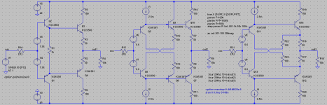
Not to intrude, but I decided to simulate the controversial comparison.
Personally I think without proper models we're all working in the dark here. I am going to check the 1382/3503 models against the datasheet next.
I've added my own modification to the circuit to the comparison and according to LTSpice, it has about half the distortion of the diamond buffer. I don't see any problem with the extra current draw through the OP devices here. Also, notice that if you increase the current sources to 7.5mA, THD gets dramatically worse. In light of this, I changed the 500 ohm resistor to 1k so the drivers would have about the same bias current between the three circuits.
The diamond buffer does seem to have much more linear input impedance.
I modified the circuit so you can run a transient analysis at any frequency you desire for ten cycles by only modifying the F1 parameter. AC analysis makes things look very good, but I had a rude awakening when I tried to run my Allison deviations at 60MHz before making the modifications I have. It might be educational to look at the HF behavior of these circuits in transient analysis.
- keantoken
Attachments
Not to intrude, but I decided to simulate the controversial comparison.
Personally I think without proper models we're all working in the dark here. I am going to check the 1382/3503 models against the datasheet next.
I've added my own modification to the circuit to the comparison and according to LTSpice, it has about half the distortion of the diamond buffer. I don't see any problem with the extra current draw through the OP devices here. Also, notice that if you increase the current sources to 7.5mA, THD gets dramatically worse.
Again, unless you do it like Andy above, I don't think these simulations are really meaningful in the context of a CFA. BTW, the YAP IPS runs at 1.2mA. The VAS is at 10mA.
double EF vs diamond
Absolutely! I also simmed both circuits (a useless exercise btw, as these circuits are barely related to the real YAP) and what did I get?.........
With the KSA1381/KSC3503 models (from Fairchild) Andy's bootstrapped diamond IPS was better.
BUT.... with 2SA1381/2SC3503 models (also from Fairchild) Glen's double EF IPS was better, at least if R14=R15=0, otherwise you'll get a complete different picture.
Indeed, no real problems. But you need low distortion current sources, as now they are part of the signal path. If the OPS is configured as to have some voltage gain (see Glen's circuit on post #186, for example) you can simply replaces the current sources by only four resistors, see: http://www.diyaudio.com/forums/showpost.php?p=1682224&postcount=254
BTW, do we really need a simulator to figure that out?
Cheers,
Edmond.
edit: For protection of the two input trannies and better step response, I recommend the addition of two diodes as shown in:
http://home.tiscali.nl/data.odyssey/images/AMP23-pub-OPS-L.PNG D11 and D12
Not to intrude, but I decided to simulate the controversial comparison.
Personally I think without proper models we're all working in the dark here.
Absolutely! I also simmed both circuits (a useless exercise btw, as these circuits are barely related to the real YAP) and what did I get?.........
With the KSA1381/KSC3503 models (from Fairchild) Andy's bootstrapped diamond IPS was better.
BUT.... with 2SA1381/2SC3503 models (also from Fairchild) Glen's double EF IPS was better, at least if R14=R15=0, otherwise you'll get a complete different picture.
I am going to check the 1382/3503 models against the datasheet next.
I've added my own modification to the circuit to the comparison and according to LTSpice, it has about half the distortion of the diamond buffer. I don't see any problem with the extra current draw through the OP devices here.
Indeed, no real problems. But you need low distortion current sources, as now they are part of the signal path. If the OPS is configured as to have some voltage gain (see Glen's circuit on post #186, for example) you can simply replaces the current sources by only four resistors, see: http://www.diyaudio.com/forums/showpost.php?p=1682224&postcount=254
Obviously ! and a much higher impedance as well.[snip]
The diamond buffer does seem to have much more linear input impedance.
[snip]
- keantoken
BTW, do we really need a simulator to figure that out?
Cheers,
Edmond.
edit: For protection of the two input trannies and better step response, I recommend the addition of two diodes as shown in:
http://home.tiscali.nl/data.odyssey/images/AMP23-pub-OPS-L.PNG D11 and D12
Last edited:
Not to intrude, but I decided to simulate the controversial comparison.
The diamond buffer does seem to have much more linear input impedance.
That point is obvious and has never been denied. See post 160:
http://www.diyaudio.com/forums/showpost.php?p=1904702&postcount=160
However, how much of an impact this has on the overall linearity of a complete VFB amplifier incorporating one such CFB OPS is something you’ll need to simulate a complete VFB amplifier incorporating one such CFB OPS to find out
On your output stage R141 is 1k what power rating is this.
I'm using 1W. It would dissipade only under critical conditions (heavy clipping, protection activated).
Indeed, no real problems. But you need low distortion current sources, as now they are part of the signal path.
Well, I'm inclined to think the experienced designers here know about this, but just for the heck of increasing transistor count, why not try this CCS? Someone posted it in one of the CCS threads... By tweaking R2 and R6, I found it somehow fun to make this design work far better than I would expect in real life.
In simulation, it does very well without any adjustment. If you mess with R2 and R6 (in AC analysis), you will notice that you can cause the output to turn 180 degrees - which means the CCS is now overcompensating. By tweaking these resistors, you can make response smoothly 90 degrees across spectrum, which means that any current error is mostly harmonics (I'm sure I'm right on this).
I wouldn't expect it to stay adjusted so well with respect to temperature coefficients and all those nasty real-life things. Theoretically drift will cause there to be a bottom limit beyond which adjustment is useless. I wonder what this limit is? I would simulate with the .temp command, but I don't know whether to trust the models.
Notes:
1: The 2N5769/5771 are only 15V transistors. I would suggest replacing the output transistors with C1845/A992 if you need higher voltage (in the simulator this works well, at least).
2: C1 and C2 are effectively miller compensation to smooth out response peaking, which I added because they would actually ring from pulses (I think this circuit uses EC as well as NFB which would explain the overcompensation trick).
3: The diodes can be safely ignored. They were an experiment with pulse response.
4: I include my modifications of the models for the 2N5771/5769 in the .asc file. I modified the models to fit the datasheets much better, though Sawreyrw tells me they're wrong somehow (I still don't know what he means). You may substitute models if you want, but these models are the ones I tweaked with and if you change them the adjustment will be thrown off.
I know that I'm outdone in this thread with respect to experience and skill in design, but it's my loss if I don't post my thoughts and learn more myself. So please be tolerant of any obvious mistakes I make.
- keantoken
Attachments
Last edited:
One Question Goes to Admin
I know I may get banned from here because of the below .
However, all subscribed users will know my opinion at least.
During my stay at this forum, I Found many many useful technical information’s, Rich of documents, Rich of details. Knowledge Base let say.
No one denies that all of the information’s in here *even* the forum itself is a live because of the members. Who gave there time and effort to this place.
And some people with some serious experience solid knowledge, has been (Banned), (Account Disabled), (Or some thing else)
They might did something wrong, I don’t know.
But at least diyAudio as it looks, they don’t appreciate there time and there efforts, the information’s they gave to this place, that made other people to join, Even some of those members (Donated) to this place.
I wish the Admin of this site will give an answer to this situation.
Because whatever they did, I don’t think they deserve this end. none of them.
Thanks
- Status
- This old topic is closed. If you want to reopen this topic, contact a moderator using the "Report Post" button.
- Home
- Amplifiers
- Solid State
- YAP power amp revisited, now at v2.1