Correction to my post #636:
The beefy wire leads of the Nichicon Muse KZ actually DO FIT through the holes in this PCB. I discovered that I had a teeny tiny bit of solder left in one of the holes, which my desoldering braid had not quite picked up first pass. Anyway, after removing the solder speck, I got them in. Now to listen some more...
BTW Babysupra I wish you luck with your troubleshooting.
Good news on the leads fitting in the holes. When I get a plugged up hole I add solder to it and then reheat and use a spring loaded solder sucker.
I just got some low cost but nicely made CBB MKT's. They are 1uF 630v and huge. I wonder if a high dielectric strength reduces distortion? It would fit on a desktop amp but no way to go in pocket amp.
Waiting on the the results of the KZ and panasonic FR, stellar
You should get some FGs to play with and test")
I might have a play with mine and swap in some FR tomorrow.
Why does swapping the output cap make more of a difference than the input cap? (I'm assuming this since most people are playing with the outputs and not the inputs)
You should get some FGs to play with and test
I might have a play with mine and swap in some FR tomorrow.
Why does swapping the output cap make more of a difference than the input cap? (I'm assuming this since most people are playing with the outputs and not the inputs)
Last edited:
Waiting on the the results of the KZ and panasonic FR, stellar
You should get some FGs to play with and test
I might have a play with mine and swap in some FR tomorrow.
Why does swapping the output cap make more of a difference than the input cap? (I'm assuming this since most people are playing with the outputs and not the inputs)
I am putting Silmics and others on input too. However, there is real power going through the output caps (up to 50 mW). The input is a 100k with JFET so no current or power to speak of.
+1 good luck on debugging Babysupra.
Let me know if you need another PCB to retry it. I can send you a replacement for cost of shipping as I do want you to come out of this successfully. You might consider a board with all SMTs installed and tested and you just install through hole parts.
I'll check for short circuits and open circuits and go from there
And I'll switch to a 15V power supply a that is closer to the near drained 9V batteries
Could you please advise what I should read voltage wise relative to GND at each caps plus node? And also what I should read at each legs of the FETs. And also what I should read across key resistors
Thanks!
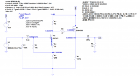
DC nominal voltages
BabySupra,
Here is what a nominal DC volts at all points should look like. It may be a little different for battery voltages and particualr JFET and MOSFETs, but not by much - maybe +/- 0.5 to 0.7v typically around the voltages in blue.
So the voltages around the JFET should be for DGS, circa 9.6v, 1.8v, 2.0v
For MOSFET DGS, circa 16,4v, 9,6v, 6.9v but in GDS pinout left to right 9.6v, 16.4v. 6.9v.
Across R3 is the voltage that tells you the bias across the JFET is 16.4-9.4v= 6.8v or 6.8mA across 1k
Across R7 is voltage that tells you the main MOSFET bias current 6.9v across 117.5R is 59mA
Voltage on inside (side facing JFET) should be 1.8v and corresponds to the DC bias setpoint on the gate of the JFET.
These are all you need to know.

The most critical ones are:
On MOSFET just these 3 measures (relative to GND) will tell you if amp is working:
1. D (pin 2 or tab) says you have the main power applied to the amp (15 to 18v)
2. G (pin 1) says the gate voltage set by JFET is working (if off then check volts across R3) (7v to 9v)
3. S (pin 3) says bias current is flowing through resistor array and you have Class A action (6v to 8v)
BabySupra,
Here is what a nominal DC volts at all points should look like. It may be a little different for battery voltages and particualr JFET and MOSFETs, but not by much - maybe +/- 0.5 to 0.7v typically around the voltages in blue.
So the voltages around the JFET should be for DGS, circa 9.6v, 1.8v, 2.0v
For MOSFET DGS, circa 16,4v, 9,6v, 6.9v but in GDS pinout left to right 9.6v, 16.4v. 6.9v.
Across R3 is the voltage that tells you the bias across the JFET is 16.4-9.4v= 6.8v or 6.8mA across 1k
Across R7 is voltage that tells you the main MOSFET bias current 6.9v across 117.5R is 59mA
Voltage on inside (side facing JFET) should be 1.8v and corresponds to the DC bias setpoint on the gate of the JFET.
These are all you need to know.
The most critical ones are:
On MOSFET just these 3 measures (relative to GND) will tell you if amp is working:
1. D (pin 2 or tab) says you have the main power applied to the amp (15 to 18v)
2. G (pin 1) says the gate voltage set by JFET is working (if off then check volts across R3) (7v to 9v)
3. S (pin 3) says bias current is flowing through resistor array and you have Class A action (6v to 8v)
Attachments
Last edited:
We are also debugging this on Head-Fi thread. A simulation with a failed-open JFET appears to give same symptoms: G and D of JFET at same voltage and S at about -3v lower due to Vgs. The MOSFET is running wide open since JFET is not pulling down the voltage at the gate.
So either bad JFET or cold solder joints on JFET S, or R4 or R5.
So either bad JFET or cold solder joints on JFET S, or R4 or R5.
Waiting on the the results of the KZ and panasonic FR, stellar
You should get some FGs to play with and test
I might have a play with mine and swap in some FR tomorrow.
Why does swapping the output cap make more of a difference than the input cap? (I'm assuming this since most people are playing with the outputs and not the inputs)
I haven't tried any electros on the input, but I would like to hear it. The capacitance needed there is so low that I figured I'd stick with film, which is usually lower distortion. There are other polyesters that could fit there, and I probably should have bought some to test. But I had to draw the line somewhere (at least for now) as my wife is already incredulous about my new cap collection...
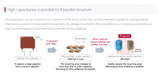
I am quite interested in trying out film caps with different dielectric materials on the input. But for the life of me I couldn't find anything besides polyester caps that would fit in that narrow space between the 3.5mm jacks. I did however, come up with a makeshift solution to cram Polyphenylene Sulfide in there. I bought four of the surface mount WIMA SMD-PPS caps, .68uF each. My plan is to stack two of them and solder leads to the ends for each channel. It'll look something like in the attached pic, (taken from the Murata website--they actually recommend doing this with their MLCCs).
I have no idea how good my silly DIY cap will sound. The individual caps are manufactured with stacked construction. PPS caps have lower distortion than polyester, but wound film caps have lower distortion than stacked. So it may be a wash... Anyway, curiosity got the better of me, so I have to try it.
Attachments
Last edited:
It turns out it was a cold solder joint on R5 that was plaguing Babysupra's amp. Although after he figured that out he accidentally installed the PSU reverse polarity and fried the MOSFETs.
It was useful to run the sims by making certain resistors infinite to simulate an open circuit of bad solder joint. Making R5 10Mohms gave same DC voltage readings of Vcc at all pins of JFET and Vcc on G and D of mosfet and 12v on S of mosfet.
It was useful to run the sims by making certain resistors infinite to simulate an open circuit of bad solder joint. Making R5 10Mohms gave same DC voltage readings of Vcc at all pins of JFET and Vcc on G and D of mosfet and 12v on S of mosfet.
oh man, the capacitor illustration with the little sweat drops are top notch, cracked me up.
Stellar, you inspired me to fill up an ebay shopping cart with caps.. :S have a US$56 cart of KZ FG and Silmics sitting there...debating whether or not to hit the checkout button lol.
X, how low could the supply voltage drop before the amp can't function properly anymore?
Stellar, you inspired me to fill up an ebay shopping cart with caps.. :S have a US$56 cart of KZ FG and Silmics sitting there...debating whether or not to hit the checkout button lol.
X, how low could the supply voltage drop before the amp can't function properly anymore?
Last edited:
I just ran a sim for the amp with a 12v supply and for high impedance 250ohm load and modest 1.4v p-p output, the distortion profile still looks fine. It only is running on 25mA bias current so don't expect it too much for large transients. At 4v p-p, the distortion starts going up like a forest of trees though. So it can work at 12v- just keep the volumes low to moderate.
X, you are kind to give so much guidance. Glad you and Babysupra got to the bottom of it.
YOB, I'm sorry to be a bad influence! Lol. If I'm not mistaken, the Panasonic FG and FR caps are just as compact as the Nichicon KA. You might consider trying the Panasonics as the main output caps paired with the smaller Silmics or KZ on bypass. I have been busy and hardly got to listen to the KZ yet, but I can say they have great resolution. .
YOB, I'm sorry to be a bad influence! Lol. If I'm not mistaken, the Panasonic FG and FR caps are just as compact as the Nichicon KA. You might consider trying the Panasonics as the main output caps paired with the smaller Silmics or KZ on bypass. I have been busy and hardly got to listen to the KZ yet, but I can say they have great resolution. .
I just realized that on simple circuits like this one, you can use LTSpice to debug by "failing" parts. Either short circuit them or make them open circuit. That's how failures usually present themselves. And if the DC setpoints match then we found the source. Very powerful tool for debugging a build gone bad.
oh man, the capacitor illustration with the little sweat drops are top notch, cracked me up.
Stellar, you inspired me to fill up an ebay shopping cart with caps.. :S have a US$56 cart of KZ FG and Silmics sitting there...debating whether or not to hit the checkout button lol.
X, how low could the supply voltage drop before the amp can't function properly anymore?
I just pulled the trigger on $120 worth of Oscons, Silmics, FC's, and Wima's.
They add up fast when you order a minimum of 10 to get a good deal.
Hi X,
I only get sound from RIGHT channel, LEFT channel is silent
new DMM readings:
M1A Pins 1 2 3: 11.9v, 18v, 9v
M1B Pins 1 2 3: 10.64v, 18v, 8.8v
Q1A: Pins G D S: 1.97v, 2.25v, 10.6v
Q1B: Pins G D S: 1.9v, 10.9v, 2.1v <--- D and S values seems opposite from Q1A!?
across R3A: 7.4v
across R3B: 7.11v
measuring across R7A 8.8v
measuring across R7B 9v
is the "B" path left channel or right channel? curious how come the JFET values for S and D are reversed between the A channel and B channel.
Hi X,
I only get sound from RIGHT channel, LEFT channel is silent
new DMM readings:
M1A Pins 1 2 3: 11.9v, 18v, 9v
M1B Pins 1 2 3: 10.64v, 18v, 8.8v
Q1A: Pins G D S: 1.97v, 2.25v, 10.6v
Q1B: Pins G D S: 1.9v, 10.9v, 2.1v <--- D and S values seems opposite from Q1A!?
across R3A: 7.4v
across R3B: 7.11v
measuring across R7A 8.8v
measuring across R7B 9v
is the "B" path left channel or right channel? curious how come the JFET values for S and D are reversed between the A channel and B channel.
Good news, we are making progress. Did you have a second board with new FETs or did you replace the MOSFETs on first board?
The JFET Q1 and Q2 are laid out in opposite orientation for convenience of routing. This is possible because the JFET is symmetric, that is D & S are interchangeable for the BF862. A very nice feature - it basically works as a gate-controlled variable resistor. So your measurements are right on the mark. From the DC setpoints data, it looks like the amp is fully functional on both channels. Bias current is a bit on high side but ok - at the max allowed thermally (76mA). Your bias currents are actually pretty well matched for both the JFETs and the MOSFETs - it should be an excellent sounding amp.
Why no music out of one channel? Possibly a bad 3.5mm stereo jack connector? I bet, if you take your DMM probe in AC volts mode and touch the S (pin 3) of the MOSFET while playing music loud on the input (assuming input jack pins are good etc), you will see fluctuating AC volts - sign of music.
When the DC setpoints are all good - the amp HAS to WORK! If no music, it is a bad connection somewhere.
These are all excellent values and means the amp should be fully working.
Code:
M1A Pins 1 2 3: 11.9v, 18v, 9v
M1B Pins 1 2 3: 10.64v, 18v, 8.8v
Q1A: Pins G D S: 1.97v, 2.25v, 10.6v
Q1B: Pins G D S: 1.9v, 10.9v, 2.1v <--- D and S values seems opposite from Q1A!?
across R3A: 7.4v
across R3B: 7.11v
measuring across R7A 8.8v
measuring across R7B 9vGood luck - you are very close. It is something like a bad cable, bad solder joint, bad jack, bad wire, etc.
It cannot be the amp.
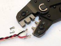
JST connector crimpers
Most of you guys probably are ok with hand soldering the 4 connector JST battery connector to the tiny 9v battery leads since you only make a couple of amps. I have been doing this by hand and believe me, it gets old after the second amp. Plus its not very sturdy, I always have to apply a small amount of solder and then use the tips of my cutters to fold and squeeze the tabs over onto the wire and insulation. A very unsatisfying and time-consuming proposition. The battery terminal wiring was perhaps the most painful step in making these amps. The rest is quite enjoyable.
Anyhow, for $23, this has all changed! I just bought the IWISS JST terminal crimpers. I wish I did this sooner. In 30 seconds, I can make a perfect beautiful professional crimp connection that folds the tabs and pierces them into the wire and the insulation to hold it all together. It is an amazing tool that really saves time if you have to do this a lot. Now that I have it, I can find uses for the small 2, 3, 4, 5 pin JST connectors for a lot of things. Like: audio in/out leads to the PCB, fans, LEDs, signal switches, power leads for batteries (like RC model LiPo battery packs), etc. The uses are endless and the connection is super secure and the connector shell and parts are very inexpensive.
Here is a photo of the first ones I crimped. It came out perfectly.
Attachments
Last edited:
- Home
- Group Buys
- xrk971 Pocket Class A Headamp GB