Today I will ask for navigation instructions to find the appropriate download aera about
www.powermodules.com
Unfortunately I am not able to find it without help.
At most websites such aeras not so easy to find like at Crown's homepage.
I need schematics of several currently available and vintage models (quickly the reference power amp 350A).
www.powermodules.com
Unfortunately I am not able to find it without help.
At most websites such aeras not so easy to find like at Crown's homepage.
I need schematics of several currently available and vintage models (quickly the reference power amp 350A).
I have two Belles 1 Series power amps; appropriately nick named "Clicker" & "Popper."
Clicker "clicks" & Popper "pops when changing surround sound decoding or some operations on DVD player.
Clicker's ser#: 134; Popper's ser#: 228. This is importan because the driver board's layouts differ considerably.
DC offset: Clicker's 33mv & -74mv; Popper's 150mv & 1.03Volts! YES you read that right 1.03V!
I sent an email to www.powermodules.com requesting a schematic though I don't it to pan out.
thanks tony
Bottom line: don't expect any schematics.
Spoke to Dave Belles himself, today. He considers schematics intellectual property & won't hand out or sell them.
If you DO get one, my PP account is ready.
Tony
Thank you for that info. This means "reverse engineering" in case of wanted schematic.
Fortunately the topology by my model "350A Reference" is easy (cascoded differential amp with current mirror and dual BjT "LM394" in the front end so as audio lateral MOSFET's from Exicon in the output).
But I don't know the exactly recommend value for the idle current. I guess 100-150mA/each Exicon MOSFET pair.
Additional an outdoor inrush current limiter is necessary to switch on six stereo devices of that model at the same time.
Belles Reverse Engineering
* using 280 schematic to help me
Unfortunately, I can't figure out what a couple of components are. One of the driver transistors has colored stripes accross it; the other, marked 41011. Can't locate info on the 41011. Started a diy thread for answers.
Can't make out what two tan colored things are, either radial caps or resistors. I expect to remove to test. Diodes have a mark or stripe at cathode end, right?
Finally I may have "bit off more than I can chew" as my EE background is limited compared to most, but that won't stop me from trying.
* appears to have 1 8099 & 2 8599s on one side; 2 8099s & 1 8599 on the other. Finishing the schematic may prove otherwise
Adjusting the Bias Of Your Amp [English]
We both love our awesome amps. I understand Belles' attitude for your late model amp. Mine are 25 years old!!
thanks for reading this far; Keep me posted on what you learn
cheers tony
Yeah, "reverse engineering." Compared to a Hafler XL-280*, the Belles is VERY simple. I scheched out the PCB on 11X17 paper & drew in the components.This means "reverse engineering" in case of wanted schematic.
* using 280 schematic to help me
Unfortunately, I can't figure out what a couple of components are. One of the driver transistors has colored stripes accross it; the other, marked 41011. Can't locate info on the 41011. Started a diy thread for answers.
Can't make out what two tan colored things are, either radial caps or resistors. I expect to remove to test. Diodes have a mark or stripe at cathode end, right?
Finally I may have "bit off more than I can chew" as my EE background is limited compared to most, but that won't stop me from trying.
Sorry I don't know what this means. But for all either of us knows, Belles may have used similar if not the same topology, just newer components in your 350! Google Rod Elliot. He does that in many of his power amps designs....topology: cascoded differential amp with current mirror
Has 3 transistors (FETs?), 8099s* & 8599s*, per side before the drivers (41011 one side, the other??); all discrete components, no chips;and dual BjT "LM394" in the front end...
* appears to have 1 8099 & 2 8599s on one side; 2 8099s & 1 8599 on the other. Finishing the schematic may prove otherwise
6 bi-polars per channel in output.audio lateral MOSFET's from Exicon in the output).
I think you guessed right. Click here for a long-winded confirmation. My Belles doesn't have a bias POT. If I can get DC offset problem licked, that should be easy. I noticed a 1 or 2 resistors w/out a "twin."But I don't know the exactly recommend value for the idle current. I guess 100-150mA/each Exicon MOSFET pair.
Adjusting the Bias Of Your Amp [English]
We both love our awesome amps. I understand Belles' attitude for your late model amp. Mine are 25 years old!!
thanks for reading this far; Keep me posted on what you learn
cheers tony
Have DC problem to trouble shoot in 2 units.
Any potentiometers on board?
Any potentiometers on board?
None! I'm certain of it. read my previous post
tony
Can you post some pictures (outside front/Rear/top view inside) ??
I cannot find any informations about the amp model "1 Series" from Power Modules/David Belles - obviously there are only few devices produced (maybe first power amp device from David Belles).
41011 sounds like custom made BjT's from RCA/Harris - check also the logo
8099/8599 could be that type:
http://www.classiccmp.org/rtellason/transdata/ksp8098.pdf
http://www.classiccmp.org/rtellason/transdata/ksp8598.pdf
http://www.datasheetcatalog.org/datasheet/motorola/MPS8598.pdf
The first steps you must perform is follow:
1) create schematic diagram
2) replace all electrolytic caps - if still DC offset present,
3) measuring of the DC conditions by shorted input and
4) starting the actually trouble shooting
concerning the not presently variable resistor: either at this place was put in a normally resistor after adjusting a potentiometer (NAD 3130 works in this kind) or an idle current servo circuit (instead a commonly used Vbe multiplier) is in use.
I guess, the topology is a normal differential input amp without current source and current mirror so as one stage VAS without Ube current source but with bootstrap cap to the output like "Citation 12"
http://www.passdiy.com/pdf/citation.pdf (Fig 7)
http://www.diyaudio.com/forums/pass-labs/173705-pass-mosfet-citation-12-clone.html
I'll post pics of PCB too-Popper partially disassembled to draw schematic.Can you post some pictures (outside front/Rear/top view inside) ??
Yeah you won't any info on Power Modules.com about these or any other pre early-mid 90s designs*. Several times a year you'll see any of these come up for auction on ebay-that's where I got Popper, my 2nd one.I cannot find any information about the amp model "1 Series" from Power Modules/David Belles - obviously there are only few devices produced (maybe first power amp device from David Belles).
* 100, 200, Class A mono blocks about 2 weeks ago, "2"-the baby brother to "1"
the 41011 is screwed to a heat sink that's then screwed to the PCB. I'll have to look on the heat sink side.41011 sounds like custom made BjT's from RCA/Harris - check also the logo
8099/8599 could be that type:
http://www.classiccmp.org/rtellason/transdata/ksp8098.pdf
http://www.classiccmp.org/rtellason/transdata/ksp8598.pdf
http://www.datasheetcatalog.org/datasheet/motorola/MPS8598.pdf
I remember a Motorola symbol on either 8099 or 8599
working on it-tough w/9 kids! I squeeze in editing (a text file)between crisses then copy/paste to a reply window.The first steps you must perform is follow:
1) create schematic diagram
Should be easy-only 3. Then check offset again? Here's where I'm fuzzy on your advice2) replace all electrolytic caps
measure w/shorted inputs (?) If offset still bad, then start the trouble shooting?If DC offset still present,
I've heard the XL280 use this*. Except for **, I do not know what any of these other terms mean. I see VAS in many other amp threads-haven't gotten to asking what it means.idle current servo circuit
Vbe multiplier
differential input amp* without current source** and current mirror...
VAS without Ube current source...bootstrap cap to the output...
I look forward to checking these links. a previous reply sent me a link that suggested info for the 41011, but no trace to its twin
I'll PM the schematic to ya.
thanks a million for your help,tony
Hi gp4Jesus,
I've repaired a few of these amps. They aren't that bad actually, and the design is relatively straight forward. Belles is being silly about his claim to "IP" for that older design, and you want the info for service reasons to repair an existing amplifier. If it makes you feel any better, he wouldn't respond to me either. Therefore I simply fixed it after recognizing the basic design elements. If I had one in front of me now, I could talk you through it.
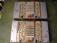
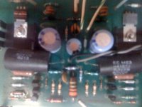
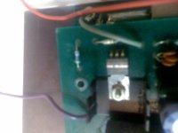
Basically, the rear PCB contains the voltage amp section. The boards mounted on the heat sinks contain the current amplifier stage and receive the two drive lines. Does that explain the connections on that cable? The transistor on the heat sink is the heat sense transistor for bias control. I have attached a couple pictures of the amp I did back in April 2006.
I didn't reverse engineer it as the amp is not that complicated. One thing you must remember when repairing amplifiers is that sometimes the amp goes DC. This will reverse bias one of the diff pair transistors and damage it. At best, the characteristics may change. Worst case, you end up with hissing, popping or intermittent open failures that cause intermittent DC offset to rail (nice eh?). Therefore, replace all pairs of transistors with matched pairs.
Note: Transistor pairs matched by measuring beta may be completely mis-matched as the temperature affects the readings a fair amount. Match transistors using a jig, basically a diff pair with current source, two matched collector loads and matched resistors from base to common. Measure between the collector loads. The better match will have a lower differential voltage.
Also, I think the predriver transistors had to be mounted differently. Look carefully at the picture of the heat sink. They are mounted on a pair of screws (hey - that's how I found the original ones mounted!). You can also see that I've cleaned the flux off the PCB. That is the only way you can check for good solder joints, solder bridges, cracked traces or poor solder wetting. If you don;t clean your flux off, those defects will be hidden from you.
-Chris
Edit: Download the pictures so you can make them larger to see more detail.
I've repaired a few of these amps. They aren't that bad actually, and the design is relatively straight forward. Belles is being silly about his claim to "IP" for that older design, and you want the info for service reasons to repair an existing amplifier. If it makes you feel any better, he wouldn't respond to me either. Therefore I simply fixed it after recognizing the basic design elements. If I had one in front of me now, I could talk you through it.
Basically, the rear PCB contains the voltage amp section. The boards mounted on the heat sinks contain the current amplifier stage and receive the two drive lines. Does that explain the connections on that cable? The transistor on the heat sink is the heat sense transistor for bias control. I have attached a couple pictures of the amp I did back in April 2006.
I didn't reverse engineer it as the amp is not that complicated. One thing you must remember when repairing amplifiers is that sometimes the amp goes DC. This will reverse bias one of the diff pair transistors and damage it. At best, the characteristics may change. Worst case, you end up with hissing, popping or intermittent open failures that cause intermittent DC offset to rail (nice eh?). Therefore, replace all pairs of transistors with matched pairs.
Note: Transistor pairs matched by measuring beta may be completely mis-matched as the temperature affects the readings a fair amount. Match transistors using a jig, basically a diff pair with current source, two matched collector loads and matched resistors from base to common. Measure between the collector loads. The better match will have a lower differential voltage.
Also, I think the predriver transistors had to be mounted differently. Look carefully at the picture of the heat sink. They are mounted on a pair of screws (hey - that's how I found the original ones mounted!). You can also see that I've cleaned the flux off the PCB. That is the only way you can check for good solder joints, solder bridges, cracked traces or poor solder wetting. If you don;t clean your flux off, those defects will be hidden from you.
-Chris
Edit: Download the pictures so you can make them larger to see more detail.
Attachments
Last edited:
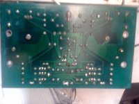
a few bad pics from a blackberry
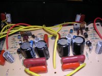
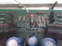
subject pretty much says it. driver board is about 98% symetrical
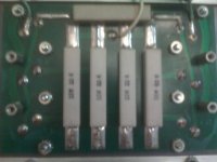
1st pic: "output board" says it. the reverse is the heat sink with the 6 devices for this channel-that's it. Don't know how this works w/5 resistors but...
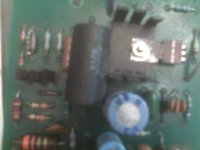
2nd pic: this half of the board connected to negative PS rail. Look carefully in upper right, you'll see the multi-colored driver transistor w/no other markings attached to a heat sink.
look to the left. Peaking around the left side of a large black bi-polar cap is the tan thing that may be a radial cap or a resistor.
just to the left of that, centered, are the MPS* 8099s & 8599s. That big resistor "divides" the negative from the positive.
* MPS-prefix of same
3rd pic: "dif transistors" a shot of both columns of MPS 8099s & 8599s
4th pic: "artwork" on the reverse side of the driver board.
anatec (Chris) your amp and mine are just different enough to tell me yours is a different model belles. my other amp's driver board is laid out differently from this one; output board is the same.
hope this helps you help me. I'll try again tomorow w/Iphone
tony
subject pretty much says it. driver board is about 98% symetrical
1st pic: "output board" says it. the reverse is the heat sink with the 6 devices for this channel-that's it. Don't know how this works w/5 resistors but...
2nd pic: this half of the board connected to negative PS rail. Look carefully in upper right, you'll see the multi-colored driver transistor w/no other markings attached to a heat sink.
look to the left. Peaking around the left side of a large black bi-polar cap is the tan thing that may be a radial cap or a resistor.
just to the left of that, centered, are the MPS* 8099s & 8599s. That big resistor "divides" the negative from the positive.
* MPS-prefix of same
3rd pic: "dif transistors" a shot of both columns of MPS 8099s & 8599s
4th pic: "artwork" on the reverse side of the driver board.
anatec (Chris) your amp and mine are just different enough to tell me yours is a different model belles. my other amp's driver board is laid out differently from this one; output board is the same.
hope this helps you help me. I'll try again tomorow w/Iphone
tony
Attachments
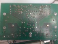
If we have the last picture (voltage amp board, solder side) in higher resolution and the according high resolution picture from the component side (top view) of that PCB, we can create the schematic diagram of that amp. It looks like a mirror symmetric topology with push-pull NPN/PNP differential input amp.
http://media.digikey.com/photos/Vishay Photos/VISHAY^SPECTROL- 043P103.jpg
BTW - the asked variable resistor (for bias resp. idle current through the last stage) is to find by picture 2 about post #12 (probably Vishay/Spectrol) und looks like this:Any potentiometers on board?
http://media.digikey.com/photos/Vishay Photos/VISHAY^SPECTROL- 043P103.jpg
Last edited:
more photos
1st pic: Hand Drawn Artwork (HDA)-approximetly to scale to 4th pic. note mostly symetrical. in next post I'll attach a scanned HDA W/components along w/a better photo of both sides of boards.
1. note left hand land area w/"+;" postive PS rail; 1, 2, & 3 - 8099, 8099, 8599 transistors respectively. #1 & 2 collector's connected to pos rail. #3 emitter connected to same. Driver transistor in upper left corner; base connected to transistor #2's collector
2. note: right hand land area w/"-;" negative PS rail; 1, 2, & 3 - 8599, 8599, 8099 transistors respectively. #1 & 2 collector's connected to neg rail. #3 emitter connected to same. Driver transistor in upper right; base connected to transistor #2's collector
3. note "~" in the middle of the middle of the pic just above small reverse "L" land area w/3 connections: Input connection
4. middle land area-larger reverse "L" shaped w/7 connections, grounded thru large 3.3 ohm resistor; input shield connected
5. resistor between the #3 transistor's bases. 2 diodes* in series connecting LH #3 base to pos rail; 2 diodes* in series connecting RH #3 base to neg rail.
* *may be Zeners
6. 3 caps, 1 polarized, between rails & inverted "U" shaped land area. note 2 ground connections near top-1 for speaker Ground, the other to PS neutral/ground
the following applies to both PS Rails and sets of transistors:
7. connections on rails (above resistors connected to #1 collectors) connected to small elbow just above #1 emiter by 2* series resistors*-one end of diode connected between them*, the other diode end connected to #2 emitter
* assume both are resistors; the first may be radial cap on Rail side. see pic w/2 collumns of transistors-tan "whatever" peeking under big black 6.3V cap. 3.3 ohm dividing view.
8. #1 & 2 emiters connected thru separate resistors to #3 collectors in OTHER set of transistors
I could include more as I have another copy of HDA with all components drawn in-makes terrible photo
9. multi colored driver off neg rail-counterpart to 41011 driver off pos rail. violet wire neg PS feed.
pic w/2 collumns of transistors. Tan whatever (Tans) peeking under big black 6.3V cap. 3.3 ohm dividing view.
Refer to note #7: Resistors closer to center than "tans," in series w/same. vertical diode between & below them.
Refer to note #5: series diodes in bottom left and right & resistor connected to #3 bases
I pray this helps you help me
tony
oops the photos
trying to do this while watching 6 kids 2 in diapers. 4th pic is MIRROR of 1st
thank
trying to do this while watching 6 kids 2 in diapers. 4th pic is MIRROR of 1st
thank
Attachments
Last edited:
Hi gp4Jesus,
First things first.
You should have a voltage amp problem, and not an output amp problem simply due to the issues you are having there. Knowing this, just simply test the pairs of transistors and make sure they are in fact matched. The older electrolytics should be refreshed anyway, so replace them using normal, good quality parts from Digikey or wherever.
Test the current sources and other transistors. It helps to heat the transistors up while they are on the tester. Something like a Heathkit IT-18 would be your best bet for a transistor tester. You want an analog meter movement so you can see smooth trends. Matching transistors should be done with some type of jig. I think Nelson Pass has a design on his web site, Walter Jung may have as well. I have one I use that differs a bit.
-Chris
schematic finished! No simple bias adjustment mod
Took me 4 tries to get from the 1st, confusing, lines crossed every which way, to a simple, flow, (hopefully) easy to read for some who hasn't had the hardware in front of them.
I believe one of you gurus can come up w/THE "bias solution."
I compared it to some other schematics-2 each: Hafler & Pass. I believe this design will not allow for the typical bias pot.
In the next edition I will adjust spacing in some places, complete the parts list, & post the schematic & parts list.
Just before I went to bed (@ 5am today!) I discovered the driver transistors, when viewed from "pin side," has one corner different than the other 3. W/this in mind looking @ the other, I quickly realized the "striped" driver is really the same type... UPSIDE DOWN(!) [as the other driver (041011)]
Also, in 3 places, I see 3 paralleled components w/the #15 on them & nothing else. 1 reversed polarity from the other 2. I thought they were disc caps. DMM testing reveled fixed resistance.
Next reply: schematic & parts list
Tony
Last edited:
Took me 4 tries to get from the 1st, confusing, lines crossed every which way, to a simple, flow, (hopefully) easy to read for some who hasn't had the hardware in front of them.
I believe one of you gurus can come up w/THE "bias solution."
I compared it to some other schematics-2 each: Hafler & Pass. I believe this design will not allow for the typical bias pot.
In the next edition I will adjust spacing in some places, complete the parts list, & post the schematic & parts list.
Just before I went to bed (@ 5am today!) I discovered the driver transistors, when viewed from "pin side," has one corner different than the other 3. W/this in mind looking @ the other, I quickly realized the "striped" driver is really the same type... UPSIDE DOWN(!) [as the other driver (041011)]
Also, in 3 places, I see 3 paralleled components w/the #15 on them & nothing else. 1 reversed polarity from the other 2. I thought they were disc caps. DMM testing reveled fixed resistance.
Next reply: schematic & parts list
Tony
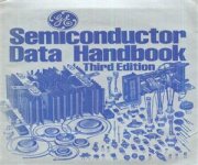
regarded the driver types "041011" and 040011 I think, the correct type is
"D41D11" and "D40D11" from
"Semiconductor Data Handbook 1977" "General Electric"
I have found this about follow URLs:
D41D11 datasheet and Application Note, Data Sheet, Circuit, PDF, Pinout | Datasheet Archive
D41D11 General Purpose PNP Output & Driver Transistor-The Electronic Goldmine
D40D datasheet and Application Note, Data Sheet, Circuit, PDF, Pinout | Datasheet Archive
in cross reference list about
http://www.kikyu.co.kr/image/uppdf/PDF200903121136.pdf
I have read this:
D40D11 2SC1014 2SC1243 D40D7
ECG210
D41D11 2SA624 2SA703 D41D7
D41D11 ECG211
D41D7 2SA624 2SA703 D41D11
but I haven't success the master resp. genuine datasheet from General Electric. Perhaps one of the members have this data book from the attachement resp. from 1977 and can scan in and posting the appropriate pages about this transistor models.
Attachments
Last edited:
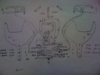
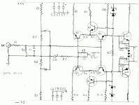
belles drawing
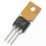
Thanks to tiefbassuebertr; you lead me to the upside down NPN driver transistor D40D13.
And now some thing to whet your appetites:Attached is a drawing I hesistate to call a schematic in fear of violating Belles IP (Intellectual property) that's about 25 years old!
some disclaimers & assumptions:
1. Q1-Q6 as the NPNs in this collection were marked on their faces "EBC."
2. EBC looking left-to-right @ the faces of Q7 & Q8.
3. I assumed the 2 diodes* connected to Q5 & Q6 were Zeners* because they looked like the 4 on either side of R23. Yes its possible I have the bias reversed, drawn based on what I interpreted as their* cathodes.
4. R12 has something in parallel w/it - markings suggest a cap. Will check the other channel for same
5. forgot to label resistors between the drivers and PS rails-let's call them R23 & R24; 100 ohms BTW
6. R15-18 same value. O O Bk gold 33 ohms I believe.
Finally I think R23 could be the "Bias" resistor.
I leave this to those w/ far more brains & experience than me.
Next post I will provide more detail w/a parts list. a couple of the resistors do not use standard color coding requiring removal to test.
Thank you all very, very much
tony
Attachments
- Status
- This old topic is closed. If you want to reopen this topic, contact a moderator using the "Report Post" button.
- Home
- Amplifiers
- Solid State
- will pay for Belles 1 Series amp info & Schematic