And you might like to reduce R2 and R9 values. This would speedup switching times of output transistors.
And in case of non-stability a cap of some 10 pF accross R6 could help.
And R15 and R16 resistors must be replaced from emitters to collectors, this is a must! Now they do not protect output during thermal runaway. After replacement they will stabilize current through output transistors.
And in case of non-stability a cap of some 10 pF accross R6 could help.
And R15 and R16 resistors must be replaced from emitters to collectors, this is a must! Now they do not protect output during thermal runaway. After replacement they will stabilize current through output transistors.
I built a bunch of these CFP amps a few years ago, they worked great.
For reference let us look at these drawings:
http://homelf.kimo.com.tw/skychutw/Circuits/DanMeyer_Tiger.jpg
Dan had several of these amps, this one was called the Little Tiger, or the Plastic Tiger(plastic 3055/2955 opts).
I used the MPS A06/A56 pair as drivers with the MJE 3055T/2955T for outputs.
Originally I used the TL072 for the opamp, but that doesn't work well. When the amp is driven into clipping the phase reverses and it sounds really, really bad. The NE5532 sounded much better and had no problems driven ino clipping.
Ideally you want the slowest opamp you can find that still sounds good, if you use a screaming fast opamp you will have stability problems when you close the loop.
I used 47 ohms for R12, 14 and 150 ohms for R15, 16 and 0.01µF for C3, 4 and 1N4148 for D2, 3
I drove the opamp right into the cathode of D2, which is also the anode of D3. I ran 4.7K bias resistors from the bases of Q5, 6 (the driver transistors) to the ±15V opamp supply rails.
Initially I used an 18-0-18 80VA transformer, but went to 20-0-20 160VA later on.
The 20-0-20 160VA transformer had a lower no-load voltage (because of better transformer regulation), and sounded vastly better.
The main filter caps for a stereo amp were only 3300µF + 47µF + 0.1µF, OK for 40hz, and we had a subwoofer also.
I was able to squeeze two channels of the power amp with all supply parts (except the transformer), a pair of 7815/7915 regs, a 1*C fan cooled sink, pre-amp, 24dB crossover, headphone amp, and an image processor, all into a 4.5" X 5.5" X 1" package.
Thanks everyone for the suggestions.
I am not sure what you meant by precise quiescent current setting. Need more pointers, PMA.
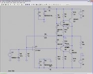
PMA, the R2/R12 and R9/R10 paires were chosen for biasing purposes. At idle, the voltage drop on R10 and R12 is about 1/2 Vbe each (that's the forward voltage drop on one of the diode). the same current going through R9 and R2 (which is twice the value of R10 and R12) is exactly one Vbe, which matches with the output devices.
Yes, I can use lower values for R2/R12 and R9/R10, but that will drop higher current out of the op-amp. I haven't gone through the datesheet for the opamp to see if that's indeed too much. I suspect 15ma (15v / 1K) for the op-amp is about right.
I had R15 and R16 originally on collector originally as sajti's scheme had suggested but decided to move it. My reasoning is that as Vbe of the output devices drop, (while maintaining the voltage drop off R2 for example), it would cause the current output from the output device to go up, which will increase voltage drop off R15, which in turns reduces the current output of the device.
Putting R15 on the collector will also work, but will a 1:2 feedback onto the emitter of the driver.
djk, I would love to see some of the schematics you had referrenced to, bu tthe link above didn't seem to produce anything, and I did a yahoo search that yielded little as well. Would you mind either posting the schematics here or giving us another link. Thanks in advance.
Again, your comments are welcome.
PMA said:Yes, now there is a voltage gain of +2 at the ouput stage.
How about precise quiescent current setting.
I am not sure what you meant by precise quiescent current setting. Need more pointers, PMA.
PMA said:And you might like to reduce R2 and R9 values. This would speedup switching times of output transistors.
PMA, the R2/R12 and R9/R10 paires were chosen for biasing purposes. At idle, the voltage drop on R10 and R12 is about 1/2 Vbe each (that's the forward voltage drop on one of the diode). the same current going through R9 and R2 (which is twice the value of R10 and R12) is exactly one Vbe, which matches with the output devices.
Yes, I can use lower values for R2/R12 and R9/R10, but that will drop higher current out of the op-amp. I haven't gone through the datesheet for the opamp to see if that's indeed too much. I suspect 15ma (15v / 1K) for the op-amp is about right.
PMA said:And R15 and R16 resistors must be replaced from emitters to collectors, this is a must! Now they do not protect output during thermal runaway.
I had R15 and R16 originally on collector originally as sajti's scheme had suggested but decided to move it. My reasoning is that as Vbe of the output devices drop, (while maintaining the voltage drop off R2 for example), it would cause the current output from the output device to go up, which will increase voltage drop off R15, which in turns reduces the current output of the device.
Putting R15 on the collector will also work, but will a 1:2 feedback onto the emitter of the driver.
djk said:I built a bunch of these CFP amps a few years ago, they worked great.
For reference let us look at these drawings:
http://homelf.kimo.com.tw/skychutw/Circuits/DanMeyer_Tiger.jpg
djk, I would love to see some of the schematics you had referrenced to, bu tthe link above didn't seem to produce anything, and I did a yahoo search that yielded little as well. Would you mind either posting the schematics here or giving us another link. Thanks in advance.
Again, your comments are welcome.
millwood,
distortion of an amplifier operated in B (AB) class can be minimalized by setting of optimal value of quiescent current for the output stage. In case that quiescent current is lower or higher than optimal value the crossover distortion will increase. Global negative feedback reduces crossover distortion, but it is not an optimal solution and especially on high frequencies crossover distortion can "colorize" the sound. It is much better to minimalize crossover distortion and not to rely only on negative feedback. This is a long story, so try to find Douglas Self Site (e.g. by Google) to learn more. Douglas Self explains this perfectly.
distortion of an amplifier operated in B (AB) class can be minimalized by setting of optimal value of quiescent current for the output stage. In case that quiescent current is lower or higher than optimal value the crossover distortion will increase. Global negative feedback reduces crossover distortion, but it is not an optimal solution and especially on high frequencies crossover distortion can "colorize" the sound. It is much better to minimalize crossover distortion and not to rely only on negative feedback. This is a long story, so try to find Douglas Self Site (e.g. by Google) to learn more. Douglas Self explains this perfectly.
I got it to output at full voltage. figured out that the problem was that the biasing resistors are just too big. so now R2=500, R12=250, and R13 remains at 1K.
current through the diodes is about 1.8ma (=(46x2-3*0.7)/(25K*2).
biasing of the driver is about 1ma.
and the gain on the op-amp is about 8x.
current through the diodes is about 1.8ma (=(46x2-3*0.7)/(25K*2).
biasing of the driver is about 1ma.
and the gain on the op-amp is about 8x.
djk said:For reference let us look at these drawings:
http://homelf.kimo.com.tw/skychutw/Circuits/DanMeyer_Tiger.jpg
I finally got it working. Here is the link:
http://home.kimo.com.tw/skychutw/Circuits/index.htm
It is under "Power-Amp/Dan Meyer".
Notice that a small resistor is placed on the emitter of the output device for all versions and for the Super Tiger it does have a small collector resistor.
The Super Tiger, also called the Tiger .01 (for the .01% IM distortion rating), sounds very good.
If you parallel another pair of outputs and raise the power supply voltage to ±52V you essentially have the early Bryston 3B.
One reason I used this output stage with voltage gain was that it gave rail-to-rail swing.
McIntosh used a similar output stage with a voltage gain of 5X in their MC502/2120/2125/2200/2205 models.
I own a pair of MC2120 that I added about $4 worth of bypass caps to, you would have to hear them to believe the sound.
millwood said:I got it to output at full voltage. figured out that the problem was that the biasing resistors are just too big. so now R2=500, R12=250, and R13 remains at 1K.
current through the diodes is about 1.8ma (=(46x2-3*0.7)/(25K*2).
biasing of the driver is about 1ma.
and the gain on the op-amp is about 8x.
Hi Millwood,
it's allways happy day, if any new circuit works well!
Now I understand the connection of biasing diodes. I recommend to remove R17. This means that the opamp will gives the bias current for the diodes. The current goes into the opamp will set the opamp's output stage into class "A", and cancel the crossover distortion.
To continue the improvment just replace the R1 with current regulator. This will reduce the load of the opamp, and results lower distortion.
And You can apply the common bypass capacitor across the bias diodes, to improve the HF response.
Sajti
sajti said:
I recommend to remove R17. This means that the opamp will gives the bias current for the diodes.
Sajti
Sajti, i am not too crazy as to set the op-amp in class A or AB (I don't believe changing the load will do that job). The use of R17 is so that the op-amp outputs (close to) zero current when there is no input signal. Otherwise, the op-amp is forced to output a signal when there is no input.
I don't know if that makes a sonic difference or not, tho.
I noticed that the circuitry has high THD as of now (0.4%). and almost all of it was generated by the op-amp,
") . Not sure why.
. Not sure why.- Status
- This old topic is closed. If you want to reopen this topic, contact a moderator using the "Report Post" button.
- Home
- Amplifiers
- Solid State
- Why wouldn't this work?