Member
Joined 2006
Thanks Junm @@
Sorry to derail it a bit..this seems to be a good makeshift for getting a flavor of how VFETs sound like..(while the power VFETs are collecting dust) ....here using a small signal 2sk79 VFET at input for voltage gain looped with a LM3886:
Amplified triode
VFET+3886 VSµç×ӹܵ¥¶Ë¼×ÀàÖÆ×÷ - 52Ó²¼þÂÛ̳ - Powered by Discuz!
Someone has tried to jack up the distortion mimicking a 2A3 SET amp distortion characteristics...
Member
Joined 2006
Here is my attempt to translate how the 2sk79 +LM3886 amp designer felt toward the amps sounding :
"Strong message of the pleasant sounding of triode existing in this amp that is this unlimited cleaniness of purity which needs to be explained with the understanding of arts" : )
"Strong message of the pleasant sounding of triode existing in this amp that is this unlimited cleaniness of purity which needs to be explained with the understanding of arts" : )
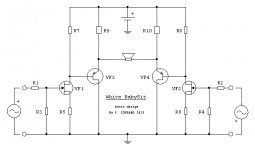
...So R1 and R5 adjusts the offset voltage and R2+R9 and R6 will do the bias current, am i right?
Not really. R1,R5 set the VFETs' Vgs i.e. their bias, but each of these resistor sets "its" VFET so they have to be adjusted in alternate steps in order to set equal currents through both VFETs and when that equilibrium is achieved, the DC offset at the output will be zero volts.
R2+R9 and R6 determine the current through the input stage and through the R1, R5 also, so that's how the value of R1,R5 is determined for wanted bias (you'll need roughly Vgs=10V for Id=1A at Vds=25V).
The schematic I drew (post #54) is optimized for 1A bias at Vds=25V and that's why the R9 is a pot - just for slight adjustment of Id equilibrium. If you want to have different bias of output stage it's better to have pots in place of R1, R5.
Member
Joined 2006
Hi Padamiecki,
Unfortunately all I know is that only 2sk79s are still available....on ebay and in Tokyo Wakamatsu.
Oh...now I remember this....
http://www.geocities.jp/mutsu562000/root/amps1/htm/hp3603.htm
Turning a compound 2sk79 +2sA1941 into a mightier J18 look alike...
An analogy to the 2sk79 + LM3886 above...
Member
Joined 2006
How about these ones?
The one with opamp in front looks interesting!
http://www.geocities.jp/mutsu562000/root/amps1/htm/hp3619.htm
The one with opamp in front looks interesting!
http://www.geocities.jp/mutsu562000/root/amps1/htm/hp3619.htm
Amplified triode
VFET+3886 VSµç×ӹܵ¥¶Ë¼×ÀàÖÆ×÷ - 52Ó²¼þÂÛ̳ - Powered by Discuz!
Someone has tried to jack up the distortion mimicking a 2A3 SET amp distortion characteristics...
Its look like a tube Buffered Gainclone....K79 SIT is a SS triode plus the LM3886 Gainclone. Well i got one similar project like this...A 6N23p +lm3886.
Thanks Juma fo clearer explanation...
The one with opamp in front looks interesting!
http://www.geocities.jp/mutsu562000/...htm/hp3619.htm
Yes, very interesting but use same rank of VFETS...the other one with Jfet inputs and lateral FET drivers also come to my mind but finding the Mosfet drivers K215/J76 are hard and most of the ones in ebay are fakes.
__________________
Member
Joined 2006
Its look like a tube Buffered Gainclone....K79 SIT is a SS triode plus the LM3886 Gainclone. Well i got one similar project like this...A 6N23p +lm3886.
This 2sk79 is no ordinary buffer and is not a cascading thing, its source and drain are actually tied to the input and output of the chipamp, steering the amp's performance which manifested in the unique distortion spectra unlike the chipamp's own : )
This 2sk79 is no ordinary buffer and is not a cascading thing, its source and drain are actually tied to the input and output of the chipamp, steering the amp's performance which manifested in the unique distortion spectra unlike the chipamp's own : )
This schematic was designed by the great Shinichi Kamijo. He call this configuration STC (Super Triode Connection)
Amplified triode.
He has made many other STC amp with Tubes.
You can view in this index page:

Contents page
Last edited:
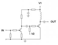
There's a loophole in that design by Mr. J. Hiraga as per ILIMZN, see post #25 of this thread. Maybe modifying the circuit may work. May those knowledgeable in modifying this will comment on how to make the circuit work with VFETS.
ILIMZN ,Juma and MOS57 or anybody out there may have an idea?
In this scheme the Vfet are used as followers and 1 ohm resistors on the drain serve to keep constant the output current (a form of autobias).
So, in particular, the circuit does not need auxiliary devices to avoid the destruction of Vfet at power on. But 60 Watt seem too optimistic and I would say impossible in Class A.
The circuit still shows the signs of aging, good transistor but today you can get better.
For some time I have in mind a scheme designed just for the Vfet.
In my mind it should have the following requirements.
- very very simple scheme
- one single power supply
- push-pull type with small or medium output power
- tracking of variations of the mains voltage (Illzman)
- balanced input
- no auxiliary circuit required To safeguard the Vfet from destruction at startup and shutdown.
- no input capacitor
- no output capacitor.
- upgradable for unbalanced input (using the new Fully Differential Phase Inverter) and also with dual power supply.
The project is currently in its infancy and did not want to present it yet but given the Vs. curiosity I might be tempted to anticipate here.

What do you think?
The conceptual scheme you see it below.
the basic idea from which I started was to explore the possibility of using the resistors as load resistors and as source resistors for providing the bias (automatic bias) to the gate.
Someone may then replace them with a pair of CCS, or a pair of inductors, for to increase the power or the efficiency of circuit, but obviously I would start with the simple resistors.
We can also decide to operate the Vfet in class A or AB.
The circuit is designed with the input Jfet of N polarity with an eye to those who want to use the 2SK79 to achieve a completely Vfet amp.
Obviously you can achieve all complementary devices: just invert the polarity of the battery.
There are no component values because we can choose them together: there are many people prepared around here.
I did a spartan simulation and the circuit seems to work, but I do not have any Vfet model for Microcap. Is there anyone who can help in this regard?
Otherwise I'll have to (or you will have to) find the time to realize the real circuit.
Comments and suggestions are always welcome.
Francesco.
Attachments
Last edited:
Michael Rothacher has done quite a bit of work modeling SITs.
Simulating SITs | Audiohobby.com
Interactive SIT Modeler | Audiohobby.com
He also has an article in Linear Audio on the topic.
Watching your project with great interest.
Juma's schematic in post #26 is really interesting for me as I have been toying with 2SK60s in a similar way.
Simulating SITs | Audiohobby.com
Interactive SIT Modeler | Audiohobby.com
He also has an article in Linear Audio on the topic.
Watching your project with great interest.
Juma's schematic in post #26 is really interesting for me as I have been toying with 2SK60s in a similar way.
Attachments
So nice to see all the renewed interest in these wonderful devices. I've had a long standing love for the Yamaha B-2 that I've had the pleasure of reconditioning a couple of and last fall I found a batter and abused B-1 that I rescued from becoming a boat anchor; both of these are nothing short of sonically incredible IMHO. I also have a set of the Sony V-FET's that I'd like to do something with at some point ... but in the mean time either of the aforementioned are such a treat to listen to.

Attachments
There's a loophole in that design by Mr. J. Hiraga as per ILIMZN, see post #25 of this thread. Maybe modifying the circuit may work. May those knowledgeable in modifying this will comment on how to make the circuit work with VFETS.
ILIMZN ,Juma and MOS57 or anybody out there may have an idea?
An externally hosted image should be here but it was not working when we last tested it.
Here is the proposed version of the Hiraga amp with NEC VFETs, which would basically stay the same regardless of which complementary VFETs were used.
The problem with it is that the bias supply is the opposing power supply rail, which means that as the Vgs of one VFET falls in order to make it conduct more and bring the output closer to the rail it's drain is tied to, the source of the opposing VFET also follows the output towards the rail which actually decreases the available negative bias supply.
If the VGS of one VFET decreases in absolute amount in order to make it conduct more, the opposing VFET's Vgs should increase in absolute amount, reducing it's conduction. This is accomplished by the relevant driver transistor conducting less, but because the opposing VFET pulls the output, and thus both sources, towards one rail, the available bias voltage for the VFET that is supposed to conduct less will decrease to a point where the driver will completely cut off, and control over that VFETs Vgs is completely lost. After that point because the available bias voltage continues to drop, the Vgs will also start dropping instead of rising, so now the VFET that is supposed to conduct less will start conducting more, resulting in cross-conduction. What is worse, this will prevent the output from reaching the desired voltage and the NFB action will attempt to correct for it by driving the originally conducting VFET even harder into conduction, actually making the problem even worse. The maximum current available for either the output or cross conduction is limited by the 1 ohm resistors in the drains of the VFETs but this does not solve the problem at all. It in fact may be possible to get complete latch-up of the circuit where it will get stuck close to one rail at the same time using the VFETs to create a near-short over both rails, and this will eventually destroy the VFETs if the resistors do not go open first.
The remedy fot his is to have extra bias supply voltage higher than the rails and tie the 8.2k resistors to them. It is also a good question what kind of frequency response one can expect from using 8.2k resistors for this purpose as this is the effective impedance of the driver, and it drives a rather large input capacitance of the NEC VFETs. To make things worse, the P and N channel NEC parts differ in input and transfer capacitances by nearly 50%. In other words, this circuit needs some work before it can be made workable.
Last edited:
The remedy fot his is to have extra bias supply voltage higher than the rails and tie the 8.2k resistors to them. It is also a good question what kind of frequency response one can expect from using 8.2k resistors for this purpose as this is the effective impedance of the driver, and it drives a rather large input capacitance of the NEC VFETs. To make things worse, the P and N channel NEC parts differ in input and transfer capacitances by nearly 50%. In other words, this circuit needs some work before it can be made workable.
So if I use k60 and J18 to this schema for example...let say extra bias supply is +/- 50v regulated and output supply at +/-25v or the same 34v, the 8.2k resistor value must be reduced or increased?
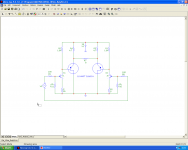
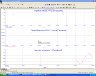
The baby is born
PSZ, thanks for the suggestion and thanks to Michael.
Yamahear, You're welcome.
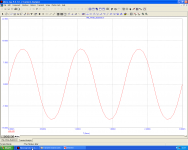
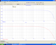
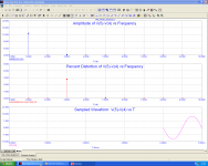
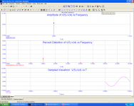
In these two days I uploaded the model of Vfet and did some simulations.
Attached are some pictures of the circuit design and the results of microcap.
Francesco
PSZ, thanks for the suggestion and thanks to Michael.
Yamahear, You're welcome.
In these two days I uploaded the model of Vfet and did some simulations.
Attached are some pictures of the circuit design and the results of microcap.
Francesco
Attachments
Looks interesting Mos57, its a balance input..is the Vfet J18 and what is the Jfet you use in the sim?
Hi, sorry I have the 2SJ28 Model only, but it is possible to use 2SJ18 in this circuit, i think.
The input Jfet is 2SK170V but 2SK369V is also very good.
- Status
- This old topic is closed. If you want to reopen this topic, contact a moderator using the "Report Post" button.
- Home
- Amplifiers
- Solid State
- What to do with this Sony V-FETS?