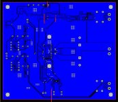
I see you tried to close the gnd-plane as much as possible. As there may circulate big ac currents through it this can cause noise on the analog input area of the pcb. For that reason on my design there is a separated AGND island on the left side, connected once via a 0R resistor with the power plane.
Last edited:
delete a loop
Thanks for suggestion, but it didn't help
chip is not damaged?
I have 2 prototypes, both identical. I was wondering if there was a wrong batch produced. I'm usually the "lucky" one if it comes to wrong batches and other hiccups. All chips were bought at Mouser, so I expect them to be genuine. I have different batch of TPA chips on hand, but I'd rather sell them than experiment further (and come back to my great sounding class AB amp)
Try grounding the TPA inputs right after their coupling caps to the AGND pin, does this help? if yes, change the WIMA for some small MLCC to test. Additionally, try grounding your existing inputs including prestage to AGND at chip and remove any GND from the input up to this point (like Star-GND)
See SLAA719:
http://www.ti.com/lit/an/slaa719/slaa719.pdf
See SLAA719:
http://www.ti.com/lit/an/slaa719/slaa719.pdf
Couldn't wait longer and made this modification. I was not courageous this time and added only 2 small Elna Silmic II 35V 100µF in //. Still much bigger than onboard 1µF ceramic. At first start the fuse of additional 12V psu blew, sign of some additional current flowing unfortunately through tpa chip. After changing to a stepped up one, the amp start to sing.I will be interested to hear from greinedo if adding a big cap to AVDD achieves even more improvement.
Definitively another improvement with those caps decoupling AVDD. There is certainly a burn in time, but right now there is already more consistent bass, more autority, improved stereo image. Seems to me more balanced and easier listening. Will listen a bit before trying to go further.
Thanks guys for these very good ideas of improvements.
Attachments
Thanks for the report. Without doing a before/after comparison myself, I think I will just go ahead and add a 1000uF/16V Nichicon HZ cap to AVDD. Or maybe two?Definitively another improvement with those caps decoupling AVDD.
And I will also use a linear regulator for the 12V rail, just not the elaborate regulator that you used!
Try grounding the TPA inputs right after their coupling caps to the AGND pin, does this help? if yes, change the WIMA for some small MLCC to test. Additionally, try grounding your existing inputs including prestage to AGND at chip and remove any GND from the input up to this point (like Star-GND)
See SLAA719:
http://www.ti.com/lit/an/slaa719/slaa719.pdf
Thank you Doctor. Noise reduced significantly. I tested it on my spare Monacor DT300 tweeter (93dB/2.83V) and now I can hear the noise from distance 20-30cm and it looks like its even better with MLCC.
Thank you Doctor. Noise reduced significantly. I tested it on my spare Monacor DT300 tweeter (93dB/2.83V) and now I can hear the noise from distance 20-30cm and it looks like its even better with MLCC.
That sounds like a serious layout issue. Beside that, the Foilcaps seem to catch up some radiated HF which gets demodulated in the front-end.
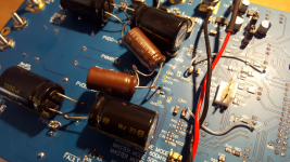
Schematic would help. May you also upload some pics of populated PCB? Is your heatsink grounded on both sides?
I don't follow - there's a mechanism for why a lower impedance on AVDD improves the SQ. What's your mechanism for more on GVDD?
This rather looks like a weak attempt to troll.
What mechanism couples supply impedance in a low current path to stereo image improvement? I never heard/seen/read of something like that.
Regarding GVDD, I refer to ripple reflection and increased dI/dT for the switching stage.
Last edited:
What mechanism couples supply impedance in a low current path to stereo image improvement? I never heard/seen/read of something like that.
So you consider something you've not heard/seen/read of not to exist?
Its clear from a few experiments with these chips (and also the TDA8932) that the analog signal processing rails do not have low enough impedance in their textbook implementation. These stages are most likely based on opamps implemented with classAB output stages - i.e. they draw a non-constant current dependent on signal and loading. Coupled with insufficient PSRR from those stages (admittedly not yet measured, but hypothesized) there's going to be signal correlated noise introduced into the music. Both L and R channels are fed from the same 'noisy' rail. See no reason that wouldn't degrade the stereo imaging?
Regarding GVDD, I refer to ripple reflection and increased dI/dT for the switching stage.
Do please explain what 'ripple reflection' means? Also what's your mechanism for this effect to influence the SQ?
Last edited:
So you consider something you've not heard/seen/read of not to exist?
That’s what you say. Your explanation is based on personal experiments, okay no problems with that. does this mean that adding capacitance to this rails (AVDD) is the proof that this particular rail isn’t low impedance enough + suffer from insufficient PSRR and the designers, considering that it’s not the first implementation they design (also on silicon level) aren’t able to do it properly while trying do be market leader and place top notch products into the market? I find it just curious how “everyone” is fixing SQ issues just with some capacitance and no vendor/designer ever sees a benefit. (Beside the fact that most “cap rollers” never do any measurements) PSRR measurements at AVDD shouldn’t be that hard to do on the EVM if adding caps is that simple anyway. if i don’t split the supply for strep sides, how can stereo image/separation get improved, the “influence” path is still there. All what happens here is to slow down the regulation bandwidth of the internal LDO and force electromigration to degrade the silicon. I wouldn’t call this a mechanism.
For the part of ripple reflection i mean it in a way that noise not only conducts this the output but also to the input (or source). That’s why switching power supplies got a filter also on the input, not only for power factor correction. The intent is to limit conducted noise getting back to the supply which here is the 12V rail (VDD). From this rail both GVDD and AVDD are supplied. GVDD here is the input of the output stage drivers, so having some more filtering here might affect noise density on the analog stage due to interference or artifacts backcoupled and demodulated. Thinking about all this, crosscoupling on silicon is something we can’t influence directly but we can limit the amount on HF getting in the IC.
For the latter, this is something that electrolytic can’t fix da es to their impedance curve which doesn’t fit well above 1MHz.
That’s what you say.
Nope, that was a question not a claim or statement. The question arises because of what I took to be an expression of disbelief from you ('anything's possible').
Your explanation is based on personal experiments, okay no problems with that. does this mean that adding capacitance to this rails (AVDD) is the proof that this particular rail isn’t low impedance enough + suffer from insufficient PSRR and the designers, considering that it’s not the first implementation they design (also on silicon level) aren’t able to do it properly while trying do be market leader and place top notch products into the market?
No, of course its not 'proof', its too early days for that. Its an interesting result which calls for further experiments. I do intend to do some in respect of the 'too low PSRR hypothesis' because to do science, all hypotheses need to be testable.
As for whether the designers 'do it properly' - it hinges on what 'properly' means. To TI, 'properly' means achieving the target measurements (THD+N in particular). However to a large number of listeners here, 'properly' means sounding as good as they can get it. No contradiction, just differing aims. So what does 'properly' mean to you?
I find it just curious how “everyone” is fixing SQ issues just with some capacitance and no vendor/designer ever sees a benefit.
Does 'everyone' in scare quotes here not really mean everyone? What benefit would a vendor/designer like to see ? I ask you because clearly you are both. Adding more capacitance on AVDD isn't going to degrade your measurements, merely give an increment on your BOM cost. But if you're a vendor defining a 'proper' design as one with certain measurements, you're not going to see any benefit of increasing your BOM.
(Beside the fact that most “cap rollers” never do any measurements) PSRR measurements at AVDD shouldn’t be that hard to do on the EVM if adding caps is that simple anyway. if i don’t split the supply for strep sides, how can stereo image/separation get improved, the “influence” path is still there. All what happens here is to slow down the regulation bandwidth of the internal LDO and force electromigration to degrade the silicon. I wouldn’t call this a mechanism.
I get the impression you've not been following along. PSRR measurements I agree aren't hard to do, just time-consuming.
For the part of ripple reflection i mean it in a way that noise not only conducts this the output but also to the input (or source). That’s why switching power supplies got a filter also on the input, not only for power factor correction.
Its me who's not following you now. Input filters are for common-mode noise suppression (if we're talking about the same input filters). Can't see how CM noise is affected here.
- Home
- Amplifiers
- Class D
- What is wrong with TPA3255?