From the datasheet, most TO-126 transistors are "optimally" biased at around 10mA. I think it is for maximum trans-conductance and linearity. But in many circuits, I often found that the optimum circuit performance (taking linearity variable out of the equation) is achieved if/such that the TO-126 in VAS position is biased with much lower current!!
So the question is how low you will allow for the bias current?
So the question is how low you will allow for the bias current?
Any particular transistor have you in mind or just the type of package?
2SA1381, 2SA1360 and the likes. I think only BD139 that is quite different from the whole bunch of TO-126 transistors
You did say "driver" transistor?
The 100 mA max. collector current of A1381/C3503 and similar CRT output transistors is a bit light for a serious audio output stage.
There are some monsters like MJE243/253 and flywweights like 2SD669/B649 or MJE340/350 and there are low voltage types like
MJE170/180, BD139/40 etc.
Some of these TO126 parts were widely used in both VAS and driver locations but they won't all fit in your 10 mA bias current frame
which I think assumes a CRT TV type.
Yes Ian, there are many types of them, including TO-220. 10mA is only a figure. The point is, if we look at the datasheet of whatever transistor, it is easy to see what is the maximum allowable current. Sometimes "optimum" current in the middle. But what defines the minimum allowable or acceptable? Pick for example 2mA for a BD139, will there be any issues? How about 1mA? Half? Something that is not detected by static analysis with simulator (and imperfect model).
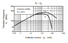
Here is the only relevant chart from one of the datasheet. But simulator will fully take care of this I believe.
A question which may arise: why not use TO-90 instead (if current needed is not so big)? That question came to me as well. But after using TO-90 and optimize, it is completely different.
Looking at the chart again, I think 2mA is still "normal"/possible with this high speed transistor. May be an issue with slower transistors. But the effect must translate to something that is recognized by simulator (OLG/stability issue, distortion, etc)
Attachments
I think there is a chart regarding linearity of hfe with Ic in some transistors. Luckily low current means low temperature. May be a +/-10% current sweep will reveal something, comparing 2mA with 6mA for example.
Naaah. There's no issue at all.
I'll ask again Jay; What do you mean here, by "driver" transistor?
At these low bias currents of maybe 2-10 mA (and since you are now considering TO92 types) you must be talking about VAS transistors instead,
or perhaps buffers for a Mosfet output stage.
In any case, the minimum bias current is dictated by the peak output current demand in class A operation. If you under-rate that, the stage
defaults to AB or C operation at higher power which is definitely not good.
In any case, the minimum bias current is dictated by the peak output current demand in class A operation. If you under-rate that, the stage
defaults to AB or C operation at higher power which is definitely not good.
Good point about class B operation. Many people ensure class A operation as much as possible in the front stages of class B amplifiers. But if the (final) distortion is low, is too much class B an issue (or audible)?
The reason I asked is because in my way to optimize a circuit, I have to cap the minimum and the maximum of certain operating points (including the currents through transistor) and then let the system solve for the maximum performance. If the objective is the final distortion at the output, the maximum result (lowest distortion) can actually come from the earlier stages operating at class B.
I don't know how for example a CFP output stage operate. The signal looks terrible (certainly not class A) but the sum at final point has no issue at all. So I think there could be nothing wrong with running VAS with so low current as long as the final result is optimum.
And that's why the question. If I have to decide on the minimum value, then what is it? 3mA? 4mA?
In "traditional" way I saw many people assign currents with "standard" proportion. But I'm not doing it like that. I just assign the current for the output stage and let the process or "algorithm" to find the rest operating points to find e.g the lowest distortion at the output.
Jay, You still won't answer which transistor you mean by "driver" so its not possible to reply without making assumptions based on your other comments.
Otherwise, any circuit based on single ended class A operation, as almost all low level discrete audio circuits are, will not tolerate insufficient bias current. There is usually an abrupt point where the output flattens out because there is insufficient current available to allow more output voltage into the load. This is likely audible, sometimes like clipping when a CCS is used.
Try it - cut your VAS bias from probably 6 mA to 2mA by changing the current source and tell us what it sounds or rather looks like at say, half and full power. Simulation will show you graphically what happens and that is the easiest way to determine the appropriate amount of bias, apart from calculation.
Note that I'm not just considering low level signals that we usually listen to. We build amplifiers rated for example, at 50W so I'm basing comments on testing at full power, 50W or the appropriate VAS output voltage to permit that. Otherwise, we will never find out what goes on by just scratching and listening on the surface of the amplifier's operation.
It doesn't matter whether you specify the output stage first or last, assume typical currents will be ok or not - it still must have sufficient bias current to ensure class A operation throughout the front end when the whole amplifier is producing full power into the worst case load you can accept. There really won't be an option for allowing some degree of non-linear operation which I inadvertently suggested by saying it degenerates to class AB then C (in hindsight this was a bad idea). Using a CCS, that change is abrupt, like clipping, and not good at all. Note that open loop gain and frequency response are affected by the bias current - further compelling reasons to get this right rather than guesstimated.
The front end of a generic 3 stage amplifier can also operate independently - just shift the feedback point from the output stage to the VAS output node and disconnect the output stage along with its bias network. Attach a 'scope and a load of 10kΩ to this point and observe the VAS output as you alter its bias current. Then increase the load by reducing the resistance to 1k, 500, even 200Ω and observe the point where bias becomes too small for linear operation.
That will be for a fixed load but the output stage is not a constant load. The bases of an EF2 output stage have a frequency dependent impedance - as low as 100Ω at high frequency for common small drivers. In the real amplifier, your VAS bias has to be increased to allow for this worst-case driver base load and the base stopper resistors of typically 100Ω help by increasing this impedance and reducing VAS loading distortion. It does mean careful consideration for the types of driver transistor that will operate with the VAS power available and it's easy to see why some designers just use triples or buffer stages to be rid of the problem. You can read all about that in Douglas Self's books or in summary, on the website.
Distortion In Power Amplifiers (see section 5.2 and also 5.4)
Jay, You still won't answer which transistor you mean by "driver" so its not possible to reply without making assumptions based on your other comments.
Thanks Ian for a lot of good info there.
Actually I don't think that the "driver" is the point, or may be my question was wrong. If you can try to imagine what I'm doing and then imagine what kind of questions that may arrive from such activities, I think that IS the between-the-line question.
So my background was doing some serious software design to optimize real world problems with Mathematical approach and dynamic programming. Hundreds of line of codes just for the Math alone.
I saw that amplifier design can also be approached from this perspective, where some variables (or range of variables) is defined and then the software is to find the optimum value for certain variable which we set as goal(s).
I don't have access to LTSpice source code (of course) but what is available with the software can be used to help do this kind of process (I'm not surprised if an expensive spice software already have that feature).
So when some variables are set, the solution is exact. Of course it is important to know which variables are to be set and with which constants and then what variable to solve.
With my pre-defined constants (or range of constants) I solve for the minimum distortion. Output current is one of the pre-defined constants and so is the output power where minimal distortion is sought after.
This process can lead to certain operating points on a TO-126 device, acting as a signal amplifying device. It can be 15mA current, or 8mA current, or 5mA current. As the objective is not distortion around the TO-126, it makes sense that 15mA doesn't have to be the solution even tho it guarantees more class-A region at that stage alone.
An alarm is "triggered" in my head when the amount of current resulting from the optimization process looks too small (as compared to my previous "standard" which is based on "taste" not Math). But I'm not sure about the exact Math to determine the minimum threshold (and that is the question).
Your mentioning about class-B operation of the TO-126 led me to check the distortion at maximum power (the optimization is based on listening level power, not maximum power, so I want to see if there is inferior performance there), but surprisingly the distortion at maximum power stands out very well, better than the comparison at lower levels.
How I determined the minimum/maximum "thresholds" for the transistor currents is mainly by looking at very good amplifiers. I haven't checked in all good amplifiers for the minimum current applied to a TO-126, but as far as I can remember I haven't seen one below 6mA (and that's also why the question arose).
May be, the subjectively lower current on the TO-126 is the consequence of my pre-defined performance of the OLG. I didn't expect the final performance is superior at all factors, only at factors that I considered important for good sound, but surprisingly it is superior anywhere I have checked. Should I be surprised? I think not. But I'm open to possible mistakes.
How I determined the minimum/maximum "thresholds" for the transistor currents is mainly by looking at very good amplifiers. I haven't checked in all good amplifiers for the minimum current applied to a TO-126, but as far as I can remember I haven't seen one below 6mA (and that's also why the question arose).
What I did was varying VAS bias current by trimmer and observed THD spectrum in ARTA in real time. That was really interesting test since any small change of VAS bias current change harmonic structure ratio accordingly. Limits were 3 mA and 24 mA, close reaching or overpassing those limits resulted in enormously higher THD. Best THD value was around 12-15 mA VAS bias current.

VAS transistors KSA1381/KSC3503.
What I did was varying VAS bias current by trimmer and observed THD spectrum in ARTA in real time. That was really interesting test since any small change of VAS bias current change harmonic structure ratio accordingly. Limits were 3 mA and 24 mA, close reaching or overpassing those limits resulted in enormously higher THD. Best THD value was around 12-15 mA VAS bias current.
How can you change only one trimmer without affecting the operation of other transistors? I mean, if increasing the VAS current lowers THD, it might be because the output transistor gets higher bias as well?
If you use CCS for the A1381, other things will be less dependent, but I don't think you use CCS for that. If you use voltage reference (TLVH431) other things will be less dependent too, but still, in many circuits (even VSSA V1.3) the currents are shared between stages.
And even if you managed to make the output bias constant, your optimal current (which happens to be the top limit) may be relevant only with certain condition (i.e. with specific components values).
But I'm glad that you think 3mA is still okay.
But I'm glad that you think 3mA is still okay.
I choose VAS current depend on VAS load. If I use 3EF, I will use 5 - 10 mA, and if 2EF I will use 6 - 15 mA, etc.
VAS current must be higher than current requirement of output stage. And some time it trade-off between THD and slew rate.
VAS current must be higher than current requirement of output stage.
Think class A... if it is collector/drain current. But if it is base/gate current...
Think class A... if it is collector/drain current. But if it is base/gate current...
Yes, it is gate/base current requierment of output stage. And if it drive high capacitance like mosfet gate, it require high current to get high slew rate. So, it depend on VAS load.
Yes, it is gate/base current requierment of output stage. And if it drive high capacitance like mosfet gate, it require high current to get high slew rate. So, it depend on VAS load.
But don't forget that the base/gate current of output stage has no direct correlation with VAS collector/drain current.
Lets look at this another way:But don't forget that the base/gate current of output stage has no direct correlation with VAS collector/drain current.
The VAS is a trans-impedance amplifier, That is, current in-voltage out. Simply, if you limit its bias current to a certain small amount, you throttle its output voltage and current into the bases of the output driver transistors. However that load is not simply resistive and varies according to signal frequency and slew rate. Overall, non-linear distortion increases as the output level, frequency or slewing are driven above the level possible with the available VAS bias current.
So, you need enough current to allow almost full rail-rail voltage swing with the type of load applied for the full audio bandwidth. The output stage is often the direct coupled load on the VAS so it it does have a direct correlation or dependency on the VAS bias current. Below the limit set by bias, it will operate normally. That implies testing at 20kHz, full power - kinda hard on amplifiers but 6-10 mA is indicative of the minimum bias in generic small-medium power amplifiers. You may be fine with much less but not at full power/bandwidth.
The output stage is often the direct coupled load on the VAS so it it does have a direct correlation or dependency on the VAS bias current.
Yes, it has dependency but I used "direct" terminology to represent a perfectly positive correlation. In Statistics (i.e. Pearson's), cofficient of correlation is given by a number (+/-) from 0 to 1. Zero means no correlation, no dependency, or random. One (1) means perfect correlation, or here I have used "direct" terminology.
Base current is a function of a lot of things. This is very important for me and I believe that more than 95% latfet amplifiers out there are designed wrongly. Why latfet? Because it has lower transconductance than other types of transistor. Even with BJT I found that designers make mistakes.
This drive current (that's what I call it) is in inverse relationship with THD, meaning that you cannot have the least distortion with the highest drive. So it is important to find out (as I have) what is the minimum drive. Then stick with the minimum drive and get the least distortion with it.
Many people just go all out for the minimum distortion, which is imo very wrong.
Let me illustrate with clear example. A 2SA1381 VAS transistor in VSSA v1.3 is biased with very high current, I think around 15 or 12mA. Jason's Peeceebee is only around 8mA. Which one drives better, or has better full blown THD20K? The higher current? No. In general Jason's circuit drive better because of the feedback (and is better overall). In VSSA v1.3 the feedback is more or less 1k/47R=21.28x. In Jason's it is 2k2/100=22x.
So this drive can be achieved using feedback. But in my approach, I have a known variable for representing this drive and it is a design objective. I achieve it as much as possible BEFORE feedback (OLG) and then get the additional amount from feedback such the total drive equal the minimum standard that I have defined.
So circuits like VSSA v1.3, with relatively low feedback, will have very low distortion, but you already know the consequences. Some people with a very low distortion system may appreciate it IF they pay attention to the effect of the low distortion. But don't forget, many others simply listen for musicality, and in this case, you might have read negative comments about such circuit, sounds "flat" etc., and it is for a very clear reason.
My own implementation of the VSSA, found by optimization using LTSpice, has lower than 8mA for the VAS but it won against both VSSA v1.3 and jason's even in the OLG. I slightly lost in THD20, because I have minimum drive requirement to fulfill.
But please, don't ask me questions. If you think I'm right, you should be able to understand what I'm talking about. If you think I'm wrong, forget about it, I'm not typical person who shares information.
ADD: BTW, I'm not saying that my circuit has worse THD because I asked for stronger drive. Actually I have lower THD because of the optimization process. If I don't care with the drive, the THD can be sub-ppm at listening level.
Last edited:
- Status
- This old topic is closed. If you want to reopen this topic, contact a moderator using the "Report Post" button.
- Home
- Amplifiers
- Solid State
- What Is The Minimum Current For TO-126 Driver?