If I like Jfet sound? I hope to find that out in the future. Have some 389/109 pairs in stock.
Bias front end: +-75% of IDSS of JFET ==> 4-5ma.
I don't know why, what is wrong with JFET input. They sound just fine, but it needs experienced ears to find out if they sound so... boring? It seems that the quality comes with the JFET used, not just how it is operated, so may be it is related to the Idss. 2SK246 is low Idss but I like them better than K170.
In general: I would like to design an amp with an open loop bandwidht of approx 40khz.
Don't you think that the goal is too pessimistic? The AC analysis chart (pic 2) does not look very good. Many circuits have flat response and zero phase shift up to 20kHz. I don't say that it matters soundwise, just cosmetically good

using as less as possible miller capacitance (this means not to high gain).
So, you are worry about miller capacitance and gain. I think the real devil is phase. From critical listening to speaker crossovers, I have learned how destructive a superposition of 2 signals with different phase can be. I believe the same thing is true with small signal in amplifier circuits. That's why non-feedback designs have their merits. I think feedback must be designed by ears, or in my case, I choose topology where feedback doesn't ruin the phase, i.e. "current feedback".
If you can buy the concept of less phase problem with current feedback, may be you can check the TSSA thread. Hahfran has posted a bipolar version if you need a "preliminary work".
This phase issue is one of a few thing that you cannot see from usual simulation.
So far, this is the best amp I ever sim'med (only reference I'm having). This VAS wsas a miracle in this design for the above points.
In term of THD? They say, once 2 trailing zeroes is achieved, it doesn't matter anymore. You're lucky that the JFET input allows for no cap in the feedback loop. In TSSA, as a consequence of "current feedback", if you had to use cap, the size will be bigger. This gives "real" distortion. May be somebody will be able to incorporate servo in the future.
In mosfet amps, low distortion usually equate to insufficient drive, and high distortion sometimes equate to sufficient drive, and higher distortion is preferable in this case (see CBS240 case with his planar stripe mosfet).
In your case, I don't know if the drive for the mosfet could be low, and if it is so then will it give bad impact or even improve things by "slowing down" the bipolar. In mosfet amps, strong drive means sonically musical and joyful, and weak drive means boring. Bipolars have very strong drive, so who knows the effect of the mosfet driver, I don't have experience with this
The AC analysis chart (pic 2) does not look very good. Many circuits have flat response and zero phase shift up to 20kHz. I don't say that it matters soundwise, just cosmetically good
Thanks for the feedback,
But please, tell me why the AC analysis looks not very good. What precisely could be better. If I compare it to other simmed amp's, this is for me one of the best.
I'm really curious.
Current feedback, well, it's a dillema for me. I've always had it difficult to choose between voltage and current feedback. And I'm not having the experience of a good listening tests beteween several amps and knowing there topology.
Maybe I go for the two options and build of both topology's, prototype amps.
Regarding the phase shift, I'm I wrong or can we see this on the AC analysis? Isn't this the group delay parameter.
It bothers me that I can't understand much of what Jay is posting.
Do you understand any, or some of it?
I had a look at your sim of open loop performance.
I see phase margin ~50degrees and gain margin ~18dB, Have I read these correctly?
I also see a steepening of the gain slope before the gain drops below +0dB. That often leads to instability.
Do you understand any, or some of it?
I had a look at your sim of open loop performance.
I see phase margin ~50degrees and gain margin ~18dB, Have I read these correctly?
I also see a steepening of the gain slope before the gain drops below +0dB. That often leads to instability.
Hi Andrew,
I understand some of it. But, as I'm a rookie, many thinks are looking or could be right for me.
Phase margin is indeed 50°, this is still enough reserve I think, even if it is sim'med. Not?
Gain margin is about 15dB Yes. Have actually not a good idea how good/bad this is. Will do some research on this topic.
I have the idea that also you would be not totaly satisied with this?
But please, tell me why the AC analysis looks not very good. What precisely could be better. If I compare it to other simmed amp's, this is for me one of the best. I'm really curious.
Sorry that I didn't pay attention to the text. Indeed it is very good. That is actually one reason why I didn't think it was an olg plot you have there. Prior to seeing your post I have seen the olg of your amp (.ASC) you posted on another thread. If I'm not mistaken that other one was not as good.
Current feedback, well, it's a dillema for me. I've always had it difficult to choose between voltage and current feedback. And I'm not having the experience of a good listening tests beteween several amps and knowing there topology.
Maybe I go for the two options and build of both topology's, prototype amps.
I don't know the "difference" between current feedback and voltage feedback myself. I just build and listen. If current feedback sounds better then I will try to find out some "explanations" as of why it sounds good (Could be right could be wrong, I'm not really into theory).
I agree. Phase distortions are quite audiable. Ears are evolved to precisely detect the locaton and relative distance to a sound source. At some time in the past, along with other reasons, it points the way to food, or the way from becoming food.... I think the real devil is phase. From critical listening to speaker crossovers, I have learned how destructive a superposition of 2 signals with different phase can be. ...
In mosfet amps, low distortion usually equate to insufficient drive, and high distortion sometimes equate to sufficient drive, and higher distortion is preferable in this case (see CBS240 case with his planar stripe mosfet).
P-ch devices tend to require more gate charge than the N-ch counterpart with similar Gm. This is why I like to drive them seperately so as each one has it's own totem pole drive as opposed to using an AC coupling cap. This is easy to do because of the Vgsth between the gates is ~7V. Mosfets are not BJT's, but in most circuits they tend to be used as such. Bob's paper addresses the need for driver current or drive charge. Keep in mind that a higher conductance device has a larger Cgs, which is usually not a problem in source follower because of the bootstrapping effect, but they also have a larger Cgd which is a problem. This capacitance is quite non-linear and must have enough drive charge to reduce the effect.
Mosfets are not BJT's, but in most circuits they tend to be used as such. Bob's paper addresses the need for driver current or drive charge. Keep in mind that a higher conductance device has a larger Cgs, which is usually not a problem in source follower because of the bootstrapping effect, but they also have a larger Cgd which is a problem. This capacitance is quite non-linear and must have enough drive charge to reduce the effect.
I believe that many design "wisdoms" were originated at era where simulators were not commonly used. At simulator era, some of the wisdom are not too "valuable" because the simulator will show them right away. What become more valuable are those still hidden from/by the simulator...
As for driver to mosfet output, Bob and many others believed that it was wrong to drive mosfet output direct from a VAS without dedicated driver. I came to the same conclusion without knowing experts opinion on this, but my conclusion was based on listening experience, not theory (so with a small sample size it could be a bad generalization).
Bensen mentioned the effect of the mosfet driver to protect the input stage (related to the impedance of the VAS I believe). AndrewT mentioned that 80deg of phase margin is good. And there is drive current issue. But I cannot put them all together to understand why direct driving from the VAS is a mistake. I mean, I don't know what parameters could be the proof of this mistake.
I have built many such circuits to proof that my listening is correct, but I'm still wondering if there is still chance for exceptions...
I have heard that one of Nelson Pass' high end amp (the X series) drive the output from VAS. He is a highly respected expert but I think he has made "mistake" before regarding to this and he might do it again.
I have also checked a few high end circuits where output is driven by VAS. What I can see is that the VAS itself is driven harder than usual. And unfortunately, I haven't heard these amplifiers.
I have tried to do the same (drive harder, add more gain stage) with my simulated amp, but only see small improvement to everything. What I'm trying to find out is why it is a mistake to drive output direct from VAS, what parameter to see. So far, what I can see is that the phase margin is not good enough (higher than 80deg).
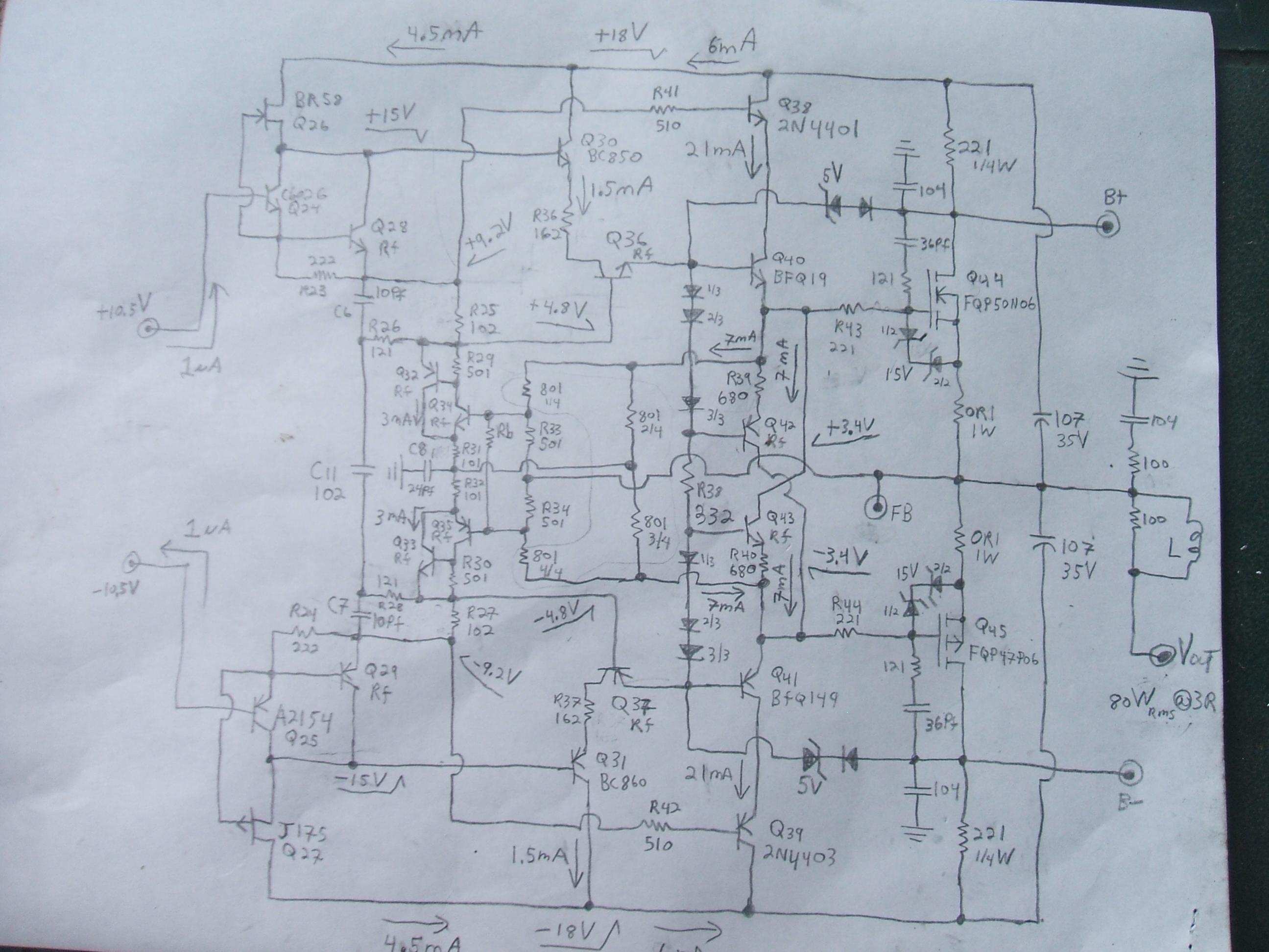
This is a circuit I made based on Bob's paper, in turn based on Dr Hawksford's work that functions very well. You can use it as a guide to build your output stage follower using vertical mosfets. Because the circuit uses local feedback/feedforward the overall linearity is very good and does not place the terrible non-linear distortion components linked to vertical 'switching' mosfets on the IPS and VAS. Also it does not require a seperate higher tier voltage supply to achieve rail to rail operation.
B+/- in this case is +/-24V. For more voltage, adjust the components to suit. Output devices can be paralelled, just use seperate gate stoppers, gate Zobel filters, and source ballast resistors.
B+/- in this case is +/-24V. For more voltage, adjust the components to suit. Output devices can be paralelled, just use seperate gate stoppers, gate Zobel filters, and source ballast resistors.
Very interesting suggestions , thanks . Just sorry for the delay, but I was quite busy with my work.
One further question: in case of very low impedance load (i.e 2 Ohm nominal, mostly inductive) and relatively low rail supply (i.e 50 V) do VMOS have advages or not?
I see that it is possible to find very high current rated ones, much more than BJTs....
One further question: in case of very low impedance load (i.e 2 Ohm nominal, mostly inductive) and relatively low rail supply (i.e 50 V) do VMOS have advages or not?
I see that it is possible to find very high current rated ones, much more than BJTs....
Advantages to what? Gm is generally high for low Vds VMOS. The lower Rds-on, the better efficiency at swtiching. Rds-on is not a factor to consider in analog applications. Cgd and Cgs is. BJT's have very high Gm but they are limited by secondary breakdown when driving highly reactive loads. Certain VMOS structures are more robust in that situation, some are not. Trench type and similar devices suffer from hot spoting and will fail in a similar fashion to secondary breakdown.
Last edited:
I mean advantages in handling very high currents per device, at low(ish) voltage They look to me that something like a 40N50 (I believe is a plabar stripe) i better suited for that than BJTs. Look s like the limitg factor is the dissipation of the case, I can't believe that a to264 can handle the rated 460 W.
Power limitation of these devices is die temperature. The faster the heat can be removed, the more power they can handle. I have mounted 1 pair of TO-220's without mica or insulation under the tab directly onto hunks of high copper brass to act as a large heat spreader or 'thermal capacitor' and cranked out over 100Wrms (resistive) from them and they did not blow up.
BJTs cannot dissipate much power at higher voltages. The depletion region between collector and base is larger at higher voltages, but small areas across this region tend to collect more electrons than others due to slight differences in doping. This can lead to thermal runaway in a localized area, called hot spotting. RETs or ring emitter transistors is an advancement that helps to nullify this by emulating a cellular structure but is only so effective. RETs tend to be faster too. Vertical mosfets that are made of a cellular structure are really many transistors in parallel. If you look at the datasheet, you will notice the temperature coefficient goes from positive (more conductance/Vgs as temp rises) to negative (less conductance/Vgs as temp rises) at high currents. If one cell conducts more current than the ones surrounding, it reaches the conductance where the coefficient is negative making it conduct less so the current must flow through the other cells. This spreads the conductance out more evenly across the die and so the die does not get hot spots. Notice higher voltage devices tend to have a larger SOA. This is because the channel length is longer and covers more die area, however transconductance is typically less for the higher voltage devices. When you factor in temperature de-rating at a die temp of 150C, the difference in SOA between higher voltage devices and lower voltage ones is much less.
Vertical mosfets are faster than laterals because the transconductance is much higher. Although BJTs have very high transconductance, the diffusion capacitance increases as it conducts more, swamping the Ft of the BJT so it actually drops at higher Ic, but effective Ft of a mosfet actually increases at higher currents because transconductance increases at higher Id. Generally speaking, Ft=(Gm/(2pi(Cgs+Cgd))) Notice, looking at the datasheet, when the device approaches Vds saturation, Cgd increases very quickly, so Ft drops accordingly. Where the current gain of a BJT drops at higher currents and can stress the driver stage, mosfets require only a little extra drive at very high currents, and virtually no extra drive at very low frequencies. There are drawbacks to using mosfets but for the vertical type high conductivity is not one of them.
500W / 2 Ohm single VMOS pair !!!
I tried today to open a new thread on the argument, but the Forum somehow "fagocitated" it
So, here we are...
I have seen with pleasure that Ixys is producing and upgrading a line of VMOS specially designed for "linear" application.
Due to a special fabrication process, they are more resistant to hot spotting i.e. seconday breackdown.
See This Article
They have an improved SOA at hot temperatures....
I want now to try out a big one like THIS
The case (SOT227)is quite unusual for Audio , it's huge , has two nice mounting holes and as a plus is alreday insulated.
I believe that this would be the only case that can realistically transfer the 750 W that the device is rated. The same device exists in standard TO 264
and it is rated even more (short of 1KW) but I find diffcult to implement an efficient dissipator for it.
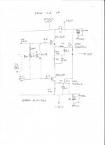
So I would like to make an OP lite the one in the sketch (sorry, I am away from my Eagle), for a subwoofer use, 500W / 2 Ohm continuos duty.
In know that I am under the 1/4 power rule (I am actually at 1/3) but I believe the case makes the difference.
Look at the 75C (case T) SOA graphs, very promising.
Any comments?
I tried today to open a new thread on the argument, but the Forum somehow "fagocitated" it
So, here we are...
I have seen with pleasure that Ixys is producing and upgrading a line of VMOS specially designed for "linear" application.
Due to a special fabrication process, they are more resistant to hot spotting i.e. seconday breackdown.
See This Article
They have an improved SOA at hot temperatures....
I want now to try out a big one like THIS
The case (SOT227)is quite unusual for Audio , it's huge
, has two nice mounting holes and as a plus is alreday insulated.I believe that this would be the only case that can realistically transfer the 750 W that the device is rated. The same device exists in standard TO 264
and it is rated even more (short of 1KW) but I find diffcult to implement an efficient dissipator for it.
So I would like to make an OP lite the one in the sketch (sorry, I am away from my Eagle), for a subwoofer use, 500W / 2 Ohm continuos duty.
In know that I am under the 1/4 power rule (I am actually at 1/3) but I believe the case makes the difference.
Look at the 75C (case T) SOA graphs, very promising.
Any comments?
Array of '240 is hardly news....
Single device has some advantages, in theory, of course.
No matching,
No current sharing,
More efficiency avoiding RSources.
Less distorsion (according to some authors)
Less circuit complication (gate stoppers / zobels - Source resistors)
Less devices, less surrounding parts, less solder joints, less possible failures.
Easy (on field...) maintenance / replacement.
About (Non Linear?) capacitance, it's about the same of 4-5 IRFP460 (or 8 /10 IRFP240).
We should manage it exactly same way, IMHO.
And if you have a look on the size (and insulation) of the SOT227, you will see that it ain't any TO3, another league.
What it retains is the possibilty to be mounted without soldering, fast replacement.
Anyone have experience with those beasts?
P.S. here's the missing sketch...
Attachments
Last edited:
in car electronics (4ohm standard impedance) we prefer parallel devices for reliability. You don't need excessive matching, in fact most high power car devices don't make matching.
For example a commercial Steg K2-04 (italian) get +1.5kW @4ohm with 7 pairs of IRF640 and goes up to 2ohm BTL.
For 1kW/4ohm you don't need 10 pairs of IRFP240...but, if you want, you always get half input capacitance of IXYS.
For "non linear" capacitance i mean vs Vds.
So, not easy to drive.
Anyway, everything can be done. The difference is the final result.
In past i've done some sims with quasi FDP61N20 with poor results, so i've stop the research.
Single device is opposite of reliability for high power use. If the single isn't perfect part, perfect mounting..how long can survive?
Over car, PA gets more devices.
ps: if you want easy replace, get TO3 sockets eheheheeheheh Plug&Play
OK, OK, OK
I got your point.
You , like thousands before use 5+ pairs.
There is pleanty of experience on that.
Got it.
Move on.
BTW, I use sockets on TO3s from more than 20 Years hehehehehehehe
You smile less when you have to demount/remount 24 devices (+ insulators and eventual thermal compound) on field to troubleshoot.
Last edited:
- Status
- This old topic is closed. If you want to reopen this topic, contact a moderator using the "Report Post" button.
- Home
- Amplifiers
- Solid State
- Vertical MOSFETs for a PA amplifier OP