If you do not put drivers on main heatsink, then any random change in air temperature gradient inside amplifier changes idle current. Tried on many development samples. You need defined temperature (of all components that influence idle current) to monitor and control. The only way to do so is to put drivers, output devices and sensor transistor onto same heatsink.
This "CFP" bias has higher dV/dT compared to standard circuit. I have designed it during PA2/PA4 development. With conventional circuit, I measured quite different idle current for cold and heated amplifier. With this circuit, the difference between cold start idle current and heated amplifier idle current is negligible. Drivers and the BD135 are on the same heatsink with output devices.
Regarding reliability, no problem during 1 year operation. The trimpot is high quality multiturn Vishay-Spectrol. All bias circuit parts run at little power, no worries needed.
I thought the 135 was the OPS device , is PA2/4 a triple ? .. I saw the PA4 w/ 8 ops's on your site (pix not clear - no schema). They were huge HS's on the prototypes.

It is just a design "rule" for the Vbe to collapse to class B with wiper failure. One could just parallel a 3.7V Zener/ 4-5 diodes/or blue led across Vbe as backup.
OS
If you do not put drivers on main heatsink, then any random change in air temperature gradient inside amplifier changes idle current. Tried on many development samples. You need defined temperature (of all components that influence idle current) to monitor and control. The only way to do so is to put drivers, output devices and sensor transistor onto same heatsink.
Exactly that's what I wanted to tell but especially on this forum you can find some very self-confident people.
If you do not put drivers on main heatsink, then any random change in air temperature gradient inside amplifier changes idle current. Tried on many development samples. You need defined temperature (of all components that influence idle current) to monitor and control. The only way to do so is to put drivers, output devices and sensor transistor onto same heatsink.
How do the OEM's get away with this , then ??
Just about all the japanese receivers use separate driver-heatsink scheme. AKSA uses separates on his 55's and 100's. Carlos's DX's , all separate drivers. I have not etched yet , so I am still open to this.To better understand , if the ambient temp changes on a separate driver/ heatsink arrangement , that would increase Ic in the outputs (creating heat).
Would not this also be compensated for by the Vbe ? , even as it does not monitor the driver gain/temp. ? A "thermal "lag" time might be created , but would this not be ultimately compensated for ?
OS
Have you checked if the amp is oscillating ? That can make the bias circuit ineffective when the amp reaches a certain temperature.
Nope , Cold zoble - CRO shows nothing. I mis-read a pair of IPS resistors once to get a oscillator , Vbias would not adjust at high bias , became tame at 70ma and below. (a Valid symptom/problem concerning faulty Vbe response).
Even at 200ma/device , blowing on the bias generator lowers the bias very quickly. (with a hair dryer)
OS
Last edited:
This circuit helps to get almost zero tempco of idle current:
I really like this circuit now ...
LT shows VERY tight idle current vs. frequency/ or amplitude with it. (below - r25 IS THE 500r trimmer).I will take the "leap of faith" . If I understood correctly , the ksc3503-N channel goes to the heatsink , but the P-channel (KSA1381) stays on the PCB. What would be the ambient effect on it (the P- channel ??)
You confirm this will compensate a EF2 with "all" (driver/outputs) on the main HS ??? It will just take 5 minutes to back those drivers up to the main heatsink again ... I have mastered sprint layout ( 400 boards and more to come).
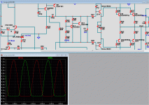
83ma @ 100hz /84ma @ 1k/ 81ma@20k/ 78ma @ 50K
Must see what it can do in the "real world".
OS
Attachments
Last edited:
I hope PMA's circuit works for you.
To help you with your problem, it might be a good idea to separate the problem into two parts (if there's 3 or more, then I miss them at this point because I am on my 3rd beer . . .)
1. Speed of response
2. Accuracy once Iq has stabilized.
I guess 1 is about coupling between the sensor and the heat energy emitting devices. The better the coupling the faster you should see RECOVERY from a thermal transient.
#2 is about how accurately the sensor (I include the complete sensor circuit here) can converge on the correct voltage to complete cancel the Iq error. This is about gain and initial setting.
For this reason, it may be a good idea to focus on #2 first (so use smaller output heatsinks) because what you want is accurate compensation, and then focus on #1 after that - where the priority of course will be to ensure your amp output stage remains within its thermal limits.
For what it is worth, on my amp (EF triple output), the outputs and the drivers share the same heatsink. The pre-drivers stand up in free air on the PCB. The SMD sensor is located about 1-2cms from the collector of one of the output devices.
I hope PMA's circuit works for you.
To help you with your problem, it might be a good idea to separate the problem into two parts (if there's 3 or more, then I miss them at this point because I am on my 3rd beer . . .)
1. Speed of response
2. Accuracy once Iq has stabilized.
I guess 1 is about coupling between the sensor and the heat energy emitting devices. The better the coupling the faster you should see RECOVERY from a thermal transient.
#2 is about how accurately the sensor (I include the complete sensor circuit here) can converge on the correct voltage to complete cancel the Iq error. This is about gain and initial setting.
For this reason, it may be a good idea to focus on #2 first (so use smaller output heatsinks) because what you want is accurate compensation, and then focus on #1 after that - where the priority of course will be to ensure your amp output stage remains within its thermal limits.
For what it is worth, on my amp (EF triple output), the outputs and the drivers share the same heatsink. The pre-drivers stand up in free air on the PCB. The SMD sensor is located about 1-2cms from the collector of one of the output devices.
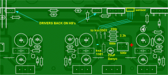
As I elaborated on above , PMA's bias gen. is just my NPN one applied to a pnp one (CFP stage). My only concern is possible "bad behavior". My KSA/C's are slightly lower gain than the BD's , but higher Vce devices. My layout will be "open ended" where I can default to a single NPN Vbe just by omitting the PNP. I WILL put the drivers back on the main HS and MAKE SURE my active sensor device is "huggin'" an output device (quick response). I wonder how you would change "sensitivity" with this CFP generator ?
As far as triples go , I LOVE Cordell's diamond triple , the predriver/driver is mounted on the same separate heatsink , they cancel each other out thermally ... leaving only the OP's Vbe to deal with.
PS - ahhh, beer is good

 , even better mixed with wine or herbs
 OS
How do the OEM's get away with this , then ??
To better understand , if the ambient temp changes on a separate driver/ heatsink arrangement , that would increase Ic in the outputs (creating heat).
Would not this also be compensated for by the Vbe ? , even as it does not monitor the driver gain/temp. ? A "thermal "lag" time might be created , but would this not be ultimately compensated for ?
OS
If the drivers are not on the heat-sink you should get over-compensation.
The Vbe multiplier is "mutiplying" for 4 Vbe junctions + 2 emitter Rs, if 2 of the junctions (the drivers) run at a fairly constant temperature then when the o/p devices get hot the Vbe mult should over compensate and reduce the bias too much.
Why not try some 0.47Ohm emitter resistors?
Self shows a "Vbe multiplication factor" variation technique to compensate for this reduced temperature coefficient in the EF case.
Brian.
Yes , reducing the sensitivity is no problem. I was able to achieve tempco with separate driver sinking. Self uses a voltage source to bias the B-E of the generator to reduce tempco. Rod elliot just recommends adjusting the ratio of current being shared between resistor divider and active device (that works well, I tried it).
Decision ,decisions ??? I really do like the drivers on the main heatsink and PMA's CFP generator. But I don't want to fail again.
OS
Decision ,decisions ??? I really do like the drivers on the main heatsink and PMA's CFP generator. But I don't want to fail again.
OS
lYes , reducing the sensitivity is no problem. I was able to achieve tempco with separate driver sinking. Self uses a voltage source to bias the B-E of the generator to reduce tempco. Rod elliot just recommends adjusting the ratio of current being shared between resistor divider and active device (that works well, I tried it).
Decision ,decisions ??? I really do like the drivers on the main heatsink and PMA's CFP generator. But I don't want to fail again.
OS
I am quite sure That Rod Elliot has a lot less problems than you because quite all his designs are CFP, so:
1) One junction less to compensate.
2) The Vbe compensation acts on the drivers only, that are on a separate H/S, if any.
Nonetheless your/his assertions about the bias network are correct.
My conclusion is that if you want to heavy bias your OP (i.e. more than 100 mA) and do not want to resort to huge H/S for reaching ROCK SOLID thermal stability you will have to use a more complex circuit than the single transistor. Your choice which one, I like the PMA's.
About where to place the drivers, I do not see any other logic solution than put them on the SAME H/S as the OP. You want to control one system, not two.
I'm going with it (the plan). Drivers back on main heatsinks and PMA's CFP generator (attachment below). I trust PMA , he suggested my dual earth return scheme and it worked beyond expectations. My concerns are that one of my sensors is out on 8cm of cable ... will the CFP "like this" ?? (parasitic oscillation).
The currents and Vce's involved are 1/100th of what a large CFP output stage has , so ... I might be over-reacting.
I could burn this off, (etch) and build it in 2-3 hours .. but I might await further feedback.
Another ???... Would a stopper resistor or cap on the ksa1381 (pcb device), be beneficial to assure stability ?
PS - I left the "door open" (layout wise), I could jumper the 220R and just omit the 1381 to have a "standard Vbe".
OS
Attachments
Last edited:
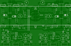
There , finished .... (below). 2 REAL bias generators and a nice layout. Looked at Rod elliots article : Compound vs Darlington
CFP VS. darlington , and he admits parasitics on the negative CFP pair. Added the cap (100-220pF) between B-C in the first device (OP sensor) - forced stability (hopefully).
OS
CFP VS. darlington , and he admits parasitics on the negative CFP pair. Added the cap (100-220pF) between B-C in the first device (OP sensor) - forced stability (hopefully).
OS
Attachments
I like it....
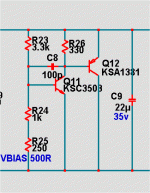
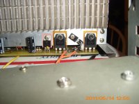
Finished PMA's "CFP" Vbias implementation (below 1). By "self heating" the heatsink with 200ma and even almost 300ma idle current I was able to eliminate "creep" and even get just a slight negative coefficient.
The finished Vbe is quite an improvement over the standard fare , I did have to play with the resistors , and using the common KSC3503/KSA1381- e gain group , the circuit's (below 2) performance and electrical characteristics should be applicable to any sink or amp (9-10ma VAS w/4 B-E's on heatsink). The PCB PNP device also compensates for the room's ambient temp. as well.
I covered up the HS convection at very high bias , Vbe dropped a mV and stabilized (NO creep , even with abuse). At normal 70mA bias, room temps between 10C and 30C had no effect on normal bias (nor at 250ma). Heating the PCB PNP collapsed the bias further (cover them vent holes). My main 3503 sensor (below 3) was mounted between the 2 njw0302's , it was very quick to respond to externally applied heating or cooling. At any time or any obscene bias , the mV's never deviated more than 2 and settled back to norm in SECONDS.
The resistor divider passes .5ma, the 3503- 2.5, and the 1381 does the most (6.8mA).
I see why this was recommended. Thanks!!
OS
Finished PMA's "CFP" Vbias implementation (below 1). By "self heating" the heatsink with 200ma and even almost 300ma idle current I was able to eliminate "creep" and even get just a slight negative coefficient.
The finished Vbe is quite an improvement over the standard fare , I did have to play with the resistors
, and using the common KSC3503/KSA1381- e gain group , the circuit's (below 2) performance and electrical characteristics should be applicable to any sink or amp (9-10ma VAS w/4 B-E's on heatsink). The PCB PNP device also compensates for the room's ambient temp. as well.I covered up the HS convection at very high bias , Vbe dropped a mV and stabilized (NO creep , even with abuse). At normal 70mA bias, room temps between 10C and 30C had no effect on normal bias (nor at 250ma). Heating the PCB PNP collapsed the bias further (cover them vent holes
). My main 3503 sensor (below 3) was mounted between the 2 njw0302's , it was very quick to respond to externally applied heating or cooling. At any time or any obscene bias , the mV's never deviated more than 2 and settled back to norm in SECONDS.The resistor divider passes .5ma, the 3503- 2.5, and the 1381 does the most (6.8mA).
I see why this was recommended. Thanks!!
OS
Attachments
Last edited:
My experimentation on this topic has lead me to the conclusion that it is most effective to compensate the pre-drivers and drivers separately from the outputs, as they have different slopes for Vbe vs. T. Mounting the pre-drivers, drivers, and a Vbe multiplier on a separate heatsink, and then using ThermalTrak output transistors and adjusting the total voltage and slope with a couple of resistors results in very tight control of bias current over temp.
Yes , the ultimate would be the Cordell diamond triple , pre/driver cancel out (use mje15032/33 for both) ... leaving just the 1 output BE to compensate for.
T-traks would be ideal for this. (my next endeavor)
This problem was one of not enough coefficient , the CFP Vbe took care of that .. I can over compensate if want. (ratio of R divider current Vs. sensor current)
OS
T-traks would be ideal for this.
(my next endeavor)This problem was one of not enough coefficient , the CFP Vbe took care of that .. I can over compensate if want. (ratio of R divider current Vs. sensor current)
OS
- Status
- This old topic is closed. If you want to reopen this topic, contact a moderator using the "Report Post" button.
- Home
- Amplifiers
- Solid State
- Vbe problems ... I'm going nuts !!