hello, what input impedance this buffer?
1Meg according to the first schematic in the first post. However that's a gate resistor and can be changed if you don't want 1Meg.
i want use ad844 with thoses.
Looks overly complex to me to run a symmetrical buffer. Given that a primary requirement is running classA, a single-ended buffer looks more appropriate.
1Meg according to the first schematic in the first post. However that's a gate resistor and can be changed if you don't want 1Meg.
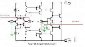
I could be wrong abraxilito, but I think he meant the input impedance of the output buffer after the TZ point, not sure if you meant that in your answer.
Cheers George
I could be wrong abraxilito, but I think he meant the input impedance of the output buffer after the TZ point, not sure if you meant that in your answer.
I could easily be mistaken here too but it looked to me that 'this buffer' referred to what was pointed to by the link following - the JLH-based buffer. Seems he wants to use that instead of your BUF03.
@donovas - yes you need to provide some kind of DC path for the JFETs, but the I/V resistor does that well enough. I'd keep the 1Meg for whenever you wish to disconnect the buffer as JFETs can be damaged by static.
no input resistor needed?
(
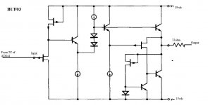
I fed my TZ direct (5mm) to input of BUF03 which has I think 50 billion ohms input impedance (5 x 10 to the 11th power) whatever it's high!!
Though it would be nice to be able to disconnect the AD's buffer so the TZ didn't have to drive both.
Cheers George
I have not used Abrxilito's dac offset nulling circuit for a while now as it is a very sensitive area to have things attached to it. I use pins 1 & 8 of the 844 if using it's buffer, or pins 1 & 5 of the BUF03 when using it.
As for the TZ resistor, I get as much gain from it as I need to get 2v with a larger resistor and a smaller cap for the low pass, as maybe a larger could cause instability in the I/V stage.
Cheers George
Yes, it's perfectly reasonable to avoid dc-offset compensation at dac output pin in order not to inject "polluted" signals, but I'm wondering if the AD844 could work at its best this way.
Original Pedja's circuit compensates prior op-amp.
This is another thing it'd be very interesting to ask Barrie Gilbert!
Just for fun
I have been changing tz resistor values with a direct connection to the input of a 250k pot on the input of my mono blocks. I started with 2.7k, then 1.5k and now I am using a 820 ohm set. It has the same great sound with all three. I did take the time to measure/look at the sin wave at 1khz at the output of tz with and without the 250k load. With the scope on the 20mvac per div and the signal adjusted on the screen to full scale(8div), I couldn't see any amplitude change between connected/disconnected with the 820 ohm set at the tZ pin 5 . I guess that this is not loading down the TZ output.
I have been changing tz resistor values with a direct connection to the input of a 250k pot on the input of my mono blocks. I started with 2.7k, then 1.5k and now I am using a 820 ohm set. It has the same great sound with all three. I did take the time to measure/look at the sin wave at 1khz at the output of tz with and without the 250k load. With the scope on the 20mvac per div and the signal adjusted on the screen to full scale(8div), I couldn't see any amplitude change between connected/disconnected with the 820 ohm set at the tZ pin 5 . I guess that this is not loading down the TZ output.
I have been changing tz resistor values with a direct connection to the input of a 250k pot on the input of my mono blocks. I started with 2.7k, then 1.5k and now I am using a 820 ohm set. It has the same great sound with all three. I did take the time to measure/look at the sin wave at 1khz at the output of tz with and without the 250k load. With the scope on the 20mvac per div and the signal adjusted on the screen to full scale(8div), I couldn't see any amplitude change between connected/disconnected with the 820 ohm set at the tZ pin 5 . I guess that this is not loading down the TZ output.
I can help explain why you got the result on the cope you describe.
May I point out, hopefully without George getting nose out of joint, that the difference between 820R and added 250K is 817R, that the difference between 2K7 and added 250K is 2K67, and likewise 1K5 is 1K49. So it is clear that there will be hardly a measured difference.
And that is what you saw on the scope.
But if instead of adding 250K with 1K5 where the Tz resistor was also 1K5, you would be the voltage on the scope to be exactly half.
It comes down to pure Ohm's Law.
And it comes down to what the nature of TZ is and that it is NOT a normal output.
So it should NOT be looked at as a normal output. In theory the TZ pin should be infinite output impedance (the ideal buffer output is supposed to be zero Ohm). In reality these are only ideal, but one is high (TZ) and the other is low (buffer).
Lets say that you measure 1V RMS signal at Tz into 1K - that means that the output is actually 1mA (0.001A). Note that it is NOT voltage but current. Hence if you increase it to 2K you will see 2V on TZ, if you increase it to 3K you will see 3V on TZ and so on. The output is always 1mA and the voltage is that current times the value of the resistor, straight Ohm's Law stuff.
Of course this means that TZ is extremely load sensitive (in voltage terms only) and whatever voltage is developed at TZ (which is a function of current times voltage) ideally needs a buffer to prevent the output moving under load. But if the load is 250K, then the 1K or 2K or 3K is only reduced by about 1% or less, so you are getting away with it and if you like what it does in the context of your system, then that is fine (of course this is an OK DIY solution, but no manufacturer would ever do it that way).
It is not a schematic that explains TZ, it is the maths and pure Ohm's Law. And just as we can have a 'voltage' output, so we can also have an unconventional 'current' output. One is very easy to understand, the other needs a different mindset but its behaviour is still explained by Ohm's Law and Thevenin's Theorem which is also related to Ohm's Law, it works with both AC and DC.
Hope this is OK with George - I am only trying to explain what you are doing and why you have the results you are getting.
Interestingly, it is not possible to overload Tz as it will produce 1mA into a dead short. It is producing zero volt, but it is designed to deliver current and it will do that into any load. It cannot be overloaded like a conventional voltage output can.
My own solution would still be a buffer as I have clients who have expectations that things should behave normally - and Tz does not do that.
To cap: Voltage output is insensitive with load as it has a low output impedance. Current out is also insensitive with load, but with respect to current which will always be 1mA no matter what the load is. The are BOTH insensitive to load, but in DIFFERENT WAYS.
And that is confusing until you actually figure it out. You can easily confirm the above by varying TZ value by 2:1 and you will see the voltage there also being 2:1 and that means the current output on TZ has not changed.
Cheers, Joe
.
Last edited:
Thanks for the info Joe. In my thinking, it would then act similarly like a CCS almost(with constant input signal). I have to believe that there must be an upper limit in the value of the resistor on TZ. The value of this resistor would then determine the gain of this circuit, there must be a limit, right? Also, the type of resistor affect the sound, if you believe resistors affect sound production. Not wanting to hijack the thread. Using a vintage RN65 mepco resistors results in the best 20/20k amplitude sweep I have seen from any player I have tested.
Thanks for the info Joe. In my thinking, it would then act similarly like a CCS almost(with constant input signal).
That is exactly how it acts, but with respect to AC (audio signal) rather than DC.
I have to believe that there must be an upper limit in the value of the resistor on TZ. The value of this resistor would then determine the gain of this circuit, there must be a limit, right?
For sure, but I have used a filter circuit at Tz and that shows/indicates it is many MegaOhm because I was able to get gains of near 80dB with it (going a bit from memory here), using around 700-800K - only using very small input signals of course on input (+) and (-) grounded.
Also, the type of resistor affect the sound, if you believe resistors affect sound production.
Got no problem with that. Just one of many things.
Cheers, Joe
.
....hi guys,ower a month ago I started to mod my rotel cd player with tda1541a dac inside.Now Im completed thead844 i/v from Pedja Rogic and build this into the player and I must say it sound incredibile good,Im amazed how this opamp can sound good if it is properly used.But I have one question for you guys,I have made the version with ad844(one piece,not stacked yet) with BF245A and 500ohm trimmer and all oder parts like by Pedja in his schematic from AYA dac.My question is,when I trim the offset with 500ohm trimmer I get the offset near the zero without a problem,but when I than check the dc on the PIN6 of the ad844 I get -10mV to -12mV .I cant get near -1,2mV like stated from some members in this tread.So my question is,is there somthing wrong with design or I do something wrong??The music play and there is no problem with the sound.Do some one have some explenation for this.

....Now Im completed thead844 i/v from Pedja Rogic and build this into the player and I must say it sound incredibile good,Im amazed how this opamp can sound good...
Only an opamp if feedback is employed.
Yes, a few mV difference is normal, even the amount you have measured is OK.
Cheers, Joe
.....hi Joe....
....thanks for your answer.Im glad to hear that the offset is OK!I have asked this becouse many mamber have stated that they mesured about -1,2mV on the PIN 6 of AD844.Have you Joe maybe some good advice for some good psu for this AD844 stage.Now Im using Dexa UWB regulators with +/-15V supply!Im thinking if theere is some bether option maybe for the power supply and if this will have big impact on the sound?
....thanks for your answer.Im glad to hear that the offset is OK!I have asked this becouse many mamber have stated that they mesured about -1,2mV on the PIN 6 of AD844.Have you Joe maybe some good advice for some good psu for this AD844 stage.Now Im using Dexa UWB regulators with +/-15V supply!Im thinking if theere is some bether option maybe for the power supply and if this will have big impact on the sound?
TDA1541A AD844

Hi, The DC offset trim is pretty sensitive. The BF245A was later changed to the 2SK170 for better stability. This might be part of the issue. With the 2SK170, allowing warm up on the TDA1541A it is possible to get -1.2 mV. I have the discrete circuit (Pedja's) here also and it behaves more or less as you describe. That I believe is a component matching issue and not having the transistors thermally connected. Back to your dac... I'd replace the BF245A with a 2SK170. Adjust the current source after the dac is warm. Adjust for zero at the input of the AD844. We only look at the output side once this is done. You might consider adding the AD844 nulling circuit. Just don't get confused when making the adjustments. I believe 20K Ohm trimmer is the correct value. The datasheet has an error. The best performance I have to date is with a triple stack with a BUF03 buffer at the TZ pin. The plain TDA1541 no A really shines with that version of the I/V. Hope that was useful.....hi guys,ower a month ago I started to mod my rotel cd player with tda1541a dac inside.Now Im completed thead844 i/v from Pedja Rogic and build this into the player and I must say it sound incredibile good,Im amazed how this opamp can sound good if it is properly used.But I have one question for you guys,I have made the version with ad844(one piece,not stacked yet) with BF245A and 500ohm trimmer and all oder parts like by Pedja in his schematic from AYA dac.My question is,when I trim the offset with 500ohm trimmer I get the offset near the zero without a problem,but when I than check the dc on the PIN6 of the ad844 I get -10mV to -12mV .I cant get near -1,2mV like stated from some members in this tread.So my question is,is there somthing wrong with design or I do something wrong??The music play and there is no problem with the sound.Do some one have some explenation for this.
....hi guys,ower a month ago I started to mod my rotel cd player with tda1541a dac inside.Now Im completed thead844 i/v from Pedja Rogic and build this into the player and I must say it sound incredibile good,Im amazed how this opamp can sound good if it is properly used.But I have one question for you guys,I have made the version with ad844(one piece,not stacked yet) with BF245A and 500ohm trimmer and all oder parts like by Pedja in his schematic from AYA dac.My question is,when I trim the offset with 500ohm trimmer I get the offset near the zero without a problem,but when I than check the dc on the PIN6 of the ad844 I get -10mV to -12mV .I cant get near -1,2mV like stated from some members in this tread.So my question is,is there somthing wrong with design or I do something wrong??The music play and there is no problem with the sound.Do some one have some explenation for this.
If you use NO coupling capacitor on output pin 6 you should adjust offset to get 0VDC at that pin, not on pin 5. If I recall correctly this was suggestion Pedja gave on his, sadly disappeared, diy pages.
If you use a output capacitor it'd be better to get 0V at pin 5.
Please report what will happen to sound with 2 and then 3 ICs stack!
Last edited:
....hi guys.....
...thanks a lot for the answers and help.I just used BF245A becouse I have this at home and just aded 4R7 resistor before DRAIN pin of BF245A like in pedjas schematics from AYA dac.Like I say before when I mesured on pin 6 I get between -10mV and -12mV,when I mesured on pin 5 I get between -1mV and -2mV.I use on pin 6 first output resistor 50ohm like by pedja and than 4,7uF output capacitor and than 100Kohm resistor from hot pin on rca to ground!!Like I say before is the totaly the same concept like by pedja in his AYA dac first editon i think.I just hope that is nothing wrong if I get some higher value of the offset seting and that this will not couse some problem to my amplifier?
The next I will try some tube buffer on pin 5 of the AD844.I have some buffer with e88cc this have 470Kohm input impedance,to hear how this will sound.
- Home
- Source & Line
- Digital Line Level
- Using the AD844 as an I/V