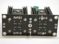
A very nice looking pcb 
A few approvements/changes till next order.
1 Make the screwholes totally insulated, remove the plating in the hole and groundplane around the hole. If you have an insulated hole you can easily use metal distances.
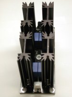
2 Insulate the heatsinks (if they aren't already), then you won't need any insulating washers.
3 The AC1 and AC2 connections are _very_ tight
I don't know how thick copper you have but maybe you should take an extra look at the pads and the size of the hot releaf bars.
A few approvements/changes till next order.
1 Make the screwholes totally insulated, remove the plating in the hole and groundplane around the hole. If you have an insulated hole you can easily use metal distances.
2 Insulate the heatsinks (if they aren't already), then you won't need any insulating washers.
3 The AC1 and AC2 connections are _very_ tight
I don't know how thick copper you have but maybe you should take an extra look at the pads and the size of the hot releaf bars.
peranders said:A very nice looking pcb
Thank you.
A few approvements/changes till next order.
1 Make the screwholes totally insulated, remove the plating in the hole and groundplane around the hole. If you have an insulated hole you can easily use metal distances.
2 Insulate the heatsinks (if they aren't already), then you won't need any insulating washers.
Both of these point are actualy already address in the design, as the copper around the hole for both the mounting posts and is not actualy connected to anything in the live part of the PCB (they are just little circles of copper, there because I liked how they looked on a PCB one of my friends did last summer). So there should be no problem using metal standoffs, or (when using the onboard heatsinks) with the diodes shorting out in the circuit.
3 The AC1 and AC2 connections are _very_ tight
I don't know how thick copper you have but maybe you should take an extra look at the pads and the size of the hot releaf bars.
Yes, that is the one thing I'm a bit upset I missed, as when I was designing the PCB I made sure everything would fit, but never thought too much about how easy it would be to push the spade terminal on with the tall heatsinks in the way. But, as you can see from the pictures, it is possible to get a crip terminal in there (and even fit on an insulating boot) and it shouldbe a bit easier with something attached to teh end of the crip terminal too.
As for the copper, the boards are 2oz with through hole plating so they should be good for the rated current, although it can make soldering some of the parts a little chalenging as there is so much heat being sucked into the board and components...
Yeah! That's what I'm talkin' 'bout. Send 'em.bigparsnip said:Wired up for mounting on an external heatsink (Rod, I guess this is how you wanted it right?), and teh diodes will need insulating if you use it like this.
----------------------------------------------------------------Basicaly, anyone who has paid me, butnot signed down for any of teh components should have their boards in the post right now(I sent them yesterday, and Royal mail says 3 days to a week to get to teh USA or Canada) so you should get them next week.
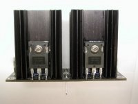
Received my borads yesterday. Looks very good. Thank you!

Got my boards yesterday Andrew, here are some pics. The only feedback so far is the mask scratches easily, especially when srubbing the board with a clean up brush, and the FET Pads are a little close. The mask is just a cosmetic issue, but the pads, I am worried about arcing due to the currents involved.
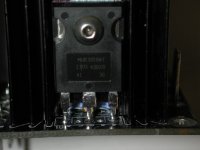
Here are some pics from he first one I built late last night. Although one of the pads appears to be shorted by a solder joint it is not as the pads are Common Cathode pads. I may actually try shaving off the unused pads under the FREDs.
You will notice I mounted the AC tabs on the bottom of the board, I did not like thier proximity to the Heat Sinks. So with an appropriate stand off, the AC in connects underneath the board, and DC on top.
Regards
Anthony
Attachments
Glad to see that people are starting to get these now, and that you got some diodes to fit in the end.
What sort of brush were you using to scrubb the boards with though, as I thought I was going to cause some damage when I was putting my first one together (the iron kept slipping of the pad and scrapping along the resist), but nothing ever happend to it (appart from the joints in question being rather poor).
Also, there are still a couple of people out there who signed down on the WIKI but who haven't been in touch yet, so if I still haven't heard from you by this Sunday night I will just assume you don't want the boards anymore and find someting else to do with them.
right, well I guess a brass brush would be kind of harsh, and I did just do a quick rather unscientific test (tried scratching the board with a knife then the Aleph-X board from the group order) and the resist is a bit softer than the x board, but I would still say that it seems more than sufficient unless you are realy giving it some abuse.
As for the pads, they had to be that close together to get the extra set in for the TO-220 devices. I can't say that I had any problems with this either, but if you need to I guess you could use a solder wick to soak up the excess solder on the joint which is causing it to flow over onto the next pad.
As for the pads, they had to be that close together to get the extra set in for the TO-220 devices. I can't say that I had any problems with this either, but if you need to I guess you could use a solder wick to soak up the excess solder on the joint which is causing it to flow over onto the next pad.
I think in general if you have enough space to mount the middle lugs on the bottom it does make fitting the cable on a lot easier, unless you are mounting the diodes on an external heatsink like Rod.
As for the max current rating of the boards, this should be just under 30A RMS (depending on what sort of diodes and hatsinks you use). however, things will get rather warm at this point, as the diodes will be right on their limit with the heatsinks I recomented (about 9deg/W) and you will need a good unrestricted airflow accross the board as well.
As for the max current rating of the boards, this should be just under 30A RMS (depending on what sort of diodes and hatsinks you use). however, things will get rather warm at this point, as the diodes will be right on their limit with the heatsinks I recomented (about 9deg/W) and you will need a good unrestricted airflow accross the board as well.
Well, on the data sheet, it states a Vf of 0.85V at a 12 amp current through one diode at 125 Degrees C. So, if you were to have say 20A RMS in total through the bridge, tihs would mean that you would have 20 X 0.85 X 0.5 = 8.5W of dissipation per device.
If you assume a room temp of 25deg, and a maximum allowable die temp of 150deg , that means you are allowed a 125 degree rise in temp, whcih would mean using a heatsink with a thermal resistance of 13deg/W (the die to chip resistance is about 1deg/W). So, you should be quite alright ussing one of the 9 deg/W heatsinks per device (this would keep the die temp down to approximately 110 degrees, but will probably be pussing things slightly in terms of getting enough cool air in to all four heatsinks once you get much past this even though in theory you should be fine up to just under 30A)
If you assume a room temp of 25deg, and a maximum allowable die temp of 150deg , that means you are allowed a 125 degree rise in temp, whcih would mean using a heatsink with a thermal resistance of 13deg/W (the die to chip resistance is about 1deg/W). So, you should be quite alright ussing one of the 9 deg/W heatsinks per device (this would keep the die temp down to approximately 110 degrees, but will probably be pussing things slightly in terms of getting enough cool air in to all four heatsinks once you get much past this even though in theory you should be fine up to just under 30A)
I guess so, but I'll have to see if there is a suitable peice of test equipment in the department here, as the nearest I think I could get these things is about 20A RMS with one of the transfomers I have (and those are at home at the minute, and I'm not sure how I would dissipate the 1600W they would chuck out  ).
).
).- Status
- This old topic is closed. If you want to reopen this topic, contact a moderator using the "Report Post" button.