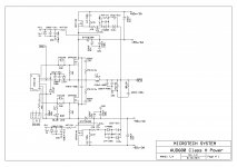
hi all good news class d with class h levels . have fun all http://www.diyaudio.com/forums/class-d/226812-my-class-d-amp-69.html#post4968835
Attachments
But WHY???
Supply pumping will pump up rail voltage to the highest possible as soon as current start to flow. This affect distortion badly and discards some part of the idle loss reduction.
The benefit of a very little higher efficiency is not too significant compared to the extra complexity, and layout is neccessarily complicated, cannot be optimized.
Many small voltage electrolytic caps are bigger and more expensive than high voltage one.
Nice experiment, good hobby, but I can't see real benefit here.
But WHY???
Supply pumping will pump up rail voltage to the highest possible as soon as current start to flow. This affect distortion badly and discards some part of the idle loss reduction.
The benefit of a very little higher efficiency is not too significant compared to the extra complexity, and layout is neccessarily complicated, cannot be optimized.
Many small voltage electrolytic caps are bigger and more expensive than high voltage one.
Nice experiment, good hobby, but I can't see real benefit here.
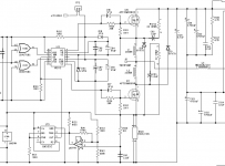
in ucd and post filter maybe , but in sigma delta and pre filter design i think it will be of great gain . using high voltage in class d is what that brings challenge. using 2 tier swing h or 3tier can make usage of +/- 180 , 120 ,60 0 , 60 ,120 , 180v possible which will yield to affordable high power with good filtering
in ucd and post filter maybe , but in sigma delta and pre filter design i think it will be of great gain . using high voltage in class d is what that brings challenge. using 2 tier swing h or 3tier can make usage of +/- 180 , 120 ,60 0 , 60 ,120 , 180v possible which will yield to affordable high power with good filtering
I dont think you understood what I wrote. Despite of the seemingly available low voltages every part of the ClassD power stage has to be dimensioned for the highest voltage, because a small output current will pump up the voltage to the highest one on the "unused" rail.
Pre or post-filter feedback is not a difference at all. Only loop gain value and loop gain stability what matter. Self-oscillating topologies are less sensitive to supply voltage variation, but still not immune. Clocked designs without error-feedforwarding are more sensitive, and the worst are clearly the open loop designs.
High voltage is actually not a problem today. There is a variety of excellent high voltage MOSFETs or IGBTs, and there is full bridge topology, SiC or hyperfast diodes to bypass FETs body diode, and BCA topology.
Simple calculations show that due to this schottky the losses nearly double. This method maybe good when using old , bad , heavy mosfets ......but why not use modern ones? Where the bodydiode makes no issues?
PS. Meanwhile there is another method of bypassing : using small inductors in drains of mosfets , instead of schottky. I think Pafi , you must know.[emoji57]
PS. Meanwhile there is another method of bypassing : using small inductors in drains of mosfets , instead of schottky. I think Pafi , you must know.[emoji57]
PS. Meanwhile there is another method of bypassing : using small inductors in drains of mosfets , instead of schottky. I think Pafi , you must know.[emoji57]
please post a diagram scheme example ,and what value is the inductor and what current should the inductor be??
Simple calculations show that due to this schottky the losses nearly double. This method maybe good when using old , bad , heavy mosfets ......but why not use modern ones? Where the bodydiode makes no issues?
Over a certain voltage you can't find really fast body diode. This voltage limit was 150V 15 years before, now somewhere around 250V, but still exists.
0.4 V drop can double conduction loss (not all losses!) if Rdson is really low (for example 0.4V/25A=16 mOhm, I wouldn't say this was typical for MOSFETs above 250V, especially at high temperature). And switching loss is always much more than this. 0.4 V drop at 100 V PS is 0.4 %, while switching loss is 5...10 %. It worth to decrease switching loss significantly at the expense of a small increasement of conduction loss, especially while EMI performance also becomes better.
PS. Meanwhile there is another method of bypassing : using small inductors in drains of mosfets , instead of schottky. I think Pafi , you must know.[emoji57]
This is the basically the same topology as the BCA, with different dimensioning. I'm not sure which is the best, all of them are usable solutions.
PS. Meanwhile there is another method of bypassing : using small inductors in drains of mosfets , instead of schottky. I think Pafi , you must know.[emoji57]
I used a variation of it 10 years ago, I combined the 2 coils into 1. (Upper coil on the attached picture.)
Attachments
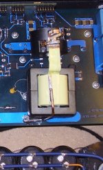
I used a variation of it 10 years ago, I combined the 2 coils into 1. (Upper coil on the attached picture.)
how was the outcome pafi??
How can you bypass bodydiode ? Please show on circuit.
http://www.diyaudio.com/forums/class-d/178317-body-diode-bypass-elegant-way.html
http://www.diyaudio.com/forums/clas...200-watts-using-2-mosfets-92.html#post2492644
http://www.diyaudio.com/forums/class-d/178317-body-diode-bypass-elegant-way-2.html#post3243499
the above links shows ways to bypass diodes

how was the outcome pafi??
With 2* STW45NM50 paralleled I tested it at 42A DC continuous in full bridge (on 0.2 ohm load), and the 10cm*20cm*4cm heat sink warmed up to about 75 C with moderate ventillation. I guess that could be about 300 W loss. Power supply voltage was 240 V in this state. If the load and power supply could have handle continuous full output voltage (but this was not a requirement) the output power could have been 180V*42A=7560W, so 300 W loss is equivalent to 4 %.
Without diode bypassing it probably would have burnt out. (At that time I couldn't buy any reasonable MOSFET with fast body diode for this high voltage.)
 wow very impressive pafi please post a schematic you used on the outputs . btw is the amp still alive today??
Sorry, I designed directly on the PCB, only very simplified schematics are drawn.
3 amp are made, 2 are still working, 1 is waiting for repair, but unfortunately nowadays I dont have any time. (Im on the forum only during public transport.)
Offtopic
 Bla-Bla
Im on the forum only during public transport.
Bla-Bla
Last edited:
- Home
- Amplifiers
- Class D
- UCD 25 watts to 1200 watts using 2 mosfets