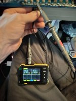
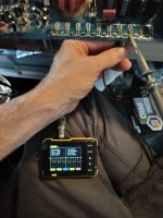
22pin driver board and Output FETs removed. Constant 12volt and 0.7 amp of current draw. Clean waves again. I probed the high side gate and got some photos.
When probing high and low side, shouldnt high and low side measure as such below or is my scope set improperly? On a x10 scale it reads 60volts at the gate, so 6volts when it should be 0v?
High Side
gate Leg 1:nothing
drain Leg 2positive rail
source Leg 3:nothing
Low side
Leg 1:negative rail
Leg 2:nothing
Leg 3:negative rail
Attachments
You should leave your scope on DC coupling. You lose too much valuable information on AC coupling.
Have you ever viewed the square wave on the outputs of an amplifier with this scope? Was it a perfect square wave?
What's important is the gate to source voltage. I don't know why the high-side gate is at 60v.
If the relay is engaging, connect a load across the speaker terminals and re-check as you are now.
With or without a load, place the ground on the source terminal and the probe tip on the gate. Connecting across the 100k pulldown resistor is the same (as far as connections are concerned).
The relay is engaging. power suppply side is fine. With the 22pin driver board in place but none of the outpet FETs, on outputs I do not see a sqaure wave, while ground is source and probe is on gate.
Under this condition the power supply functions normally.
When output FETs are in the board the power supply drive wave is funky looking and serious voltage drop as well as excessive current draw heating the PS mostfets. Same applies for 1 mosfet in place for both the high and low side on both sides of the board. Ruling out bad output mosfets.
What actually occured was that i had negative ground source on the main negative of the amp and I had probed the gate to the output FET nearest to the rail caps, which caused sparks to fly. Prior to this the board was running fine.
Im beginning to think the ICs of the 22pin pin board shorted
Last edited:
While it's possible that the ICs have failed, it's not likely since they're so well isolated from the output transistors. It's more likely that the driver transistors have failed.
Have you checked all of the driver transistors on that board?
Also check all of the 1k and 470 ohm resistors between the driver transistors and the transistors mentioned below.
As a side note, any time you get one of these driver boards to repair, you should blindly replace Q7, 11, 19 and 22. They very commonly fail, even though they check as being OK.
If you remove the output transistors and drive a signal into the amp, do you have a drive on the gate pads of any of the output transistors?
The very first thing i did when this happened was replace the driver transistors with brand new bd139/140s. I will look at 22 pin board transistors now.
I do get DC square wave on all the output fet gates when i play test tone.
I check all the 1k and 470ohm resistors on the 22 pin board and all of them are in spec.
I do get DC square wave on all the output fet gates when i play test tone.
I check all the 1k and 470ohm resistors on the 22 pin board and all of them are in spec.
Last edited:
I'm referring to the drivers on the driver board. Likely marked AG and DK.
Did you try loading the output locations (gate to source) with a capacitor (probably a 0.1uf if you're using audio to drive the amp, instead of injecting a high-frequency signal) to see if the drive signal remained OK?
Did you try loading the output locations (gate to source) with a capacitor (probably a 0.1uf if you're using audio to drive the amp, instead of injecting a high-frequency signal) to see if the drive signal remained OK?
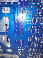
The 22 pin audio driver board.
If testing shows that the drive is OK, don't replace the drivers on the audio driver board (only 7-22 along the top edge).
If you inject a 100k signal, it will have to be beyond the crossover, at the driver board. Do you have a square wave generator? Does it produce triangle waveforms as well?
If testing shows that the drive is OK, don't replace the drivers on the audio driver board (only 7-22 along the top edge).
If you inject a 100k signal, it will have to be beyond the crossover, at the driver board. Do you have a square wave generator? Does it produce triangle waveforms as well?
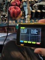
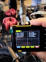
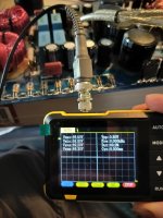
Ive placed an rca input test tone and have measured the gates of all the output transistors that are removed. The low side swings from -49v to -56v and the high swing is 45v to 53v, scope read test tone @40hz and also @ 100hz. The driver transistors seem to functioning properly.
Confirm that you read 12v from collector to collector for each emitter-follower pair of drivers on the driver board.
Since you are using a battery powered scope, you can ground to the source pad. Are all drive signals going back to within about 1v of the rail? You'll need to use DC coupling.
Are all good, clean square waves?
Since you are using a battery powered scope, you can ground to the source pad. Are all drive signals going back to within about 1v of the rail? You'll need to use DC coupling.
Are all good, clean square waves?
With ground to shunt rail, there are two ka7812 voltage regulators. one has input of 16v and output of 12v, while the other has 86volts on all connections. 86v on input, ground, and output.
Explain the last post please. Should i use the rail shunt as ground, and should i probe the collector of each two way or three way transistors?
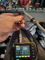
Regardless here are the waves on the gates with source as ground
Explain the last post please. Should i use the rail shunt as ground, and should i probe the collector of each two way or three way transistors?
Regardless here are the waves on the gates with source as ground
Attachments
Last edited:
The photos taken in post #35 are when i had needed to free my hand from holding the negative side to the source. Those are square waves are scoped using source and gate measures.
I rechecked data sheets for ka7812 and ka7912 and confirm that they function normally, outputting 12v.
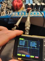
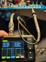
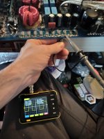
"High/Low" - "Source/Gate" photos have probed gate and source with negative on main amp negative in DC. Showing high and low voltage between gate and source on high and low sides.
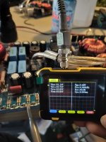
Photos of High side AC/DC have probes on source and probed at gate at 50hz
The moment I place a transistor IRF9640N in each bank of high and IRF640N on the low side, the low side 640N gate-on one side of the board - draw excessive current and cooks itself. I have replaced tranasistor from same batch twice with the same result.
"Confirm that you read 12v from collector to collector for each emitter-follower pair of drivers on the driver board." - Which transistors in question, Q7, 11, 19 and 22? Also where should i place probes? one on the collector and the other on the emitter to see 12v?
I rechecked data sheets for ka7812 and ka7912 and confirm that they function normally, outputting 12v.
"High/Low" - "Source/Gate" photos have probed gate and source with negative on main amp negative in DC. Showing high and low voltage between gate and source on high and low sides.
Photos of High side AC/DC have probes on source and probed at gate at 50hz
The moment I place a transistor IRF9640N in each bank of high and IRF640N on the low side, the low side 640N gate-on one side of the board - draw excessive current and cooks itself. I have replaced tranasistor from same batch twice with the same result.
"Confirm that you read 12v from collector to collector for each emitter-follower pair of drivers on the driver board." - Which transistors in question, Q7, 11, 19 and 22? Also where should i place probes? one on the collector and the other on the emitter to see 12v?
Attachments
-
 HIGH SIDE AC.jpg251.7 KB · Views: 11
 -
 LOW SIDE DC.jpg239.6 KB · Views: 13
 -
 HIGH SIDE DC.jpg237.4 KB · Views: 12
 -
 Low side source - (negative on main amp neg).jpg258.1 KB · Views: 14
 -
 Low side gate - (negative on main amp neg).jpg257.1 KB · Views: 11
 -
 High side Source - (negative on main amp neg).jpg256.9 KB · Views: 10
 -
 High side gate - (negative on main amp neg).jpg261.3 KB · Views: 10
 -
 LOW SIDE AC.jpg256.1 KB · Views: 12
Last edited:
I have ordered new FMU32U rectifiers, a new batch of IRF640N and IRF9640N outputs, and the PS IRFP064N transistors, starting fresh again.
Here is what i have noticed. As the board is with new PS FET, no output FET, and driver boards in. When i Go to switch on remote the voltage sags 1-2volts and draws 4 amps of current until the relay clicks on and passes voltage and current to normal 12v/1amp.
The same symptom occurs when i have previously fitted the output fets on each bank even when the relay clicks on, voltage sag and excessive current draw is still present 8.3v/4amps. \
It may just be building rail voltage, but what else would explain why it continues to occur with output FETs in place other than a shorted connection? Maybe a bad FET? Ive replaced numerous IRF640Ns.
Many amps will do strange things when starved for voltage/current.
Do you have any outputs that you could install now (even ones that previously survived)?
What power supply are your using (current rating)?
The output filter inductor could be shorted,
Did the outputs fail when clamped to the heatsink?
Do you have any outputs that you could install now (even ones that previously survived)?
What power supply are your using (current rating)?
The output filter inductor could be shorted,
Did the outputs fail when clamped to the heatsink?
- Home
- General Interest
- Car Audio
- Two Hifonics BXI-2610D, one repaired, another component ID PWN