White PCB top looks so clean and emphasize installed's parts marvelous colours. The last time I made white PCB was for ProJet Power Module in 2007.
I have in mind Upapop production....I will begin with soldering this weekend.
Marc

Sure i will, but at present i have an openloop gain of ~30dB. I would like to end up with 50 - 60dB in openloop gain.
I'm managing that kind of OLG ( 50 - 60 ) in spice by combining MF & BJT pair for o/p device. MF for i/p BJT for o/p. MF i/p in VAS gives more gain than BJT
For op amp I would try ZVN/P 3310a followed by BJT of ur choice - the 3310's have very low i/p capacitance and sound good.
mike
White PCB top looks so clean and emphasize installed's parts marvelous colours. The last time I made white PCB was for ProJet Power Module in 2007.
But possible reworks and dust later are brought to high relief, not to mention if a mistake burns something on white. White with gold designations in a clean finished project looks very posh its true.
But possible reworks and dust later are brought to high relief, not to mention if a mistake burns something on white. White with gold designations in a clean finished project looks very posh its true.
Salas, since the wite coat is only on the top side of my sigle side Pcb bord without metalised through holes, damages are not realy a issue in my case.
Marc
Last edited:
Did painted boards provide any advantage on a technical point of view ?
No Christophe, just done for personnal aesthtic pleasure.
Marc
Oh, please, never look inside one of my racks, even cd players or preamp looking from outside as they where out of the box...No Christophe, just done for personnal aesthtic pleasure

Several remarks about your reaction. (All out of topic)if you promise me to never blame my poor electronic background
- We are living in a kind of middle age, where > 90% of people using equipments don't have the slightest idea of the way they work. From cars to freezers, including mobile phones. Magic everywhere. So the ones who have a mind opened enough to try to understand them just deserve respect. And the ones who build their own ones just deserve admiration.
- I was very impressed, when young, by the culture of my parents. Old, i realize it is just a gift of the life, day after day, in response to our curiosity, no such a merit.
- The less we can do at the end of our life is to share what the life had shared with us.
- By the way, my doctor never blame-me for my poor medical background, comparing to him. On the contrary, he looks impressed by the few things i know in that domain.
This update enables TSSA BIGBT HP to be even more universal:
- serial diode MUR160 plus 22 ohm resistor in power supply rails helps to improve PSRR
- +/-OPT pins enables to connect separate power supply for the front-end (MUR160 and 22 ohm are omitted)
- power supply LED indicators for both front-end and output stage are present
- serial compensating resistor added to NTC (serves to calibrate NTC thermal response)
- serial resistors added to SK75 heatsink's GND connection (serial RC filter)
- 1 uF/63V decoupling capacitors added close to VAS transistors supply rails
- TLP627 input now accepts 12 V remote signal (serial resistor added)
- LT1034 replaced by TL431
- R2-R9 values stated for +/-50 V power supply rails
And that's about it.")
In reference to the circuit on page 16, post 159 are the TL431 the same as the Mouser parts TL431AILP Texas Instruments | Mouser ?
Also do you connect a 47R resistor from the SK75 heatsinks to ground or am I reading the circuit incorrectly. Thanks.
Did-you mean +-55V or +-27.5V ?What is the wattage at 55Vdc as I need over 150W into 4ohm speakers.
Use the Ohm law to know by yourself the power capability.
(It is better to provide tools than food to somebody suffering of salvation)
P= V²/R and V=RI, knowing that Vpeak = Vrms x 1.44. So simple.
You just have to subtract the V loss in the emitter resistance and around 3V (Collector–Emitter Saturation Voltage) in the power transistor to get the available peak voltage on your Hp terminal.
And to remember that doubling the power only increase the listening level by 3db.
Well ..150W only need +-35V peak (=24Vrms) under 4Ohm and 8.75A.
Loss in the emitter resistance will be 8.75x 0.22 -> ~2V and 3V loss in transistor -> 40V
So, this amp with +-55V will overkill your requirements.
By the way, L.C, it would be interesting that you explain to readers the principle of your nice very symmetrical complementary power transistors arrangement.
Last edited:
If you are aware of formulas, you will be aware of DIY for ever.Hi,
thanks -I am aware of the formulas etc
What I do not understand is how the output transistors work in this circuit and how to work out the SOA for the transistors.
Give-me 5 minutes, and i will try to explain this ultimatly elegant power output stage.
Last edited:
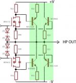
On each branch (+ and -) of the output stage are paralleled NPN and PNP power transistors.
MUR460 and MJL132A. Each one has a resistor emitter (R32, R29, R13, R15) of 0.22 Ohms.
Let-us concentrate on the upper (+V) part.
When no voltage is applied to the gate of the IRF6110, this one has infinite resistance between Drain and Source.
MUL132A base is at the +V potential via R32, so, it does not conduct.
MUR460 base is at the HP potential via R40, so, it does not conduct.
Let see whats happens when we apply some V at the IRF6110 gate. His DRAIN-SOURCE impedance will decrease. So, the V at the base of the MJL132A will decrease, and, if emitter to base is more than 0,7V, will begin to conduct.
Symmetrically, because R32 and R40 have the same values, Voltage at the base of MUR460 will increase of the same amount, and it will begin to conduct too for the same reason.
Those two transistors will be paralleled to drive the current, across their 0.22 Ohms emitter resistance to the HP charge.
The ZD zeners are here just to protect the IRF gates.
This is absolutely beautiful, because perfectly symmetrical between +V and -V half waves, whatever disparities between NPN and PNP devices.
Notice that this idea will be a perfect response if we use some Power output FET devices instead of NPN PNP, to avoid the big problem of the disparity of the capacitive holes between N and P Devices. Clever, clever, so elegant !!!!
Like all the L.C. designs.
Attachments
Last edited:
- Home
- Amplifiers
- Solid State
- TSSA - The Simplest Symmetrical Amplifier